SLUSEF1C September   2021  – June 2024 TPSM82864A , TPSM82866A

PRODMIX  

  1.   1
  2. Features
  3. Applications
  4. Description
  5. Device Options
  6. Pin Configuration and Functions
  7. Specifications
    1. 6.1 Absolute Maximum Ratings
    2. 6.2 ESD Ratings
    3. 6.3 Recommended Operating Conditions
    4. 6.4 Thermal Information
    5. 6.5 Electrical Characteristics
    6. 6.6 Typical Characteristics
  8. Detailed Description
    1. 7.1 Overview
    2. 7.2 Functional Block Diagram
    3. 7.3 Feature Description
      1. 7.3.1 Power Save Mode
      2. 7.3.2 Forced PWM Mode
      3. 7.3.3 Optimized Transient Performance from PWM to PSM Operation
      4. 7.3.4 Low Dropout Operation (100% Duty Cycle)
      5. 7.3.5 Soft Start
      6. 7.3.6 Switch Current Limit and HICCUP Short-Circuit Protection
      7. 7.3.7 Undervoltage Lockout
      8. 7.3.8 Thermal Shutdown
    4. 7.4 Device Functional Modes
      1. 7.4.1 Enable and Disable (EN)
      2. 7.4.2 Output Discharge
      3. 7.4.3 Power Good (PG)
      4. 7.4.4 Output Voltage and Mode Selection (VSET/MODE)
  9. Application and Implementation
    1. 8.1 Application Information
    2. 8.2 Typical Application
      1. 8.2.1 Design Requirements
      2. 8.2.2 Detailed Design Procedure
        1. 8.2.2.1 Setting The Output Voltage
        2. 8.2.2.2 Input and Output Capacitor Selection
      3. 8.2.3 Application Curves
    3. 8.3 Power Supply Recommendations
    4. 8.4 Layout
      1. 8.4.1 Layout Guidelines
      2. 8.4.2 Layout Examples
        1. 8.4.2.1 Thermal Considerations
  10. Device and Documentation Support
    1. 9.1 Device Support
      1. 9.1.1 Third-Party Products Disclaimer
    2. 9.2 Documentation Support
      1. 9.2.1 Related Documentation
    3. 9.3 Receiving Notification of Documentation Updates
    4. 9.4 Support Resources
    5. 9.5 Trademarks
    6. 9.6 Electrostatic Discharge Caution
    7. 9.7 Glossary
  11. 10Revision History
  12. 11Mechanical, Packaging, and Orderable Information

Package Options

Mechanical Data (Package|Pins)
Thermal pad, mechanical data (Package|Pins)
Orderable Information

Setting The Output Voltage

With the VSET/MODE pin set high or low, an adjustable output voltage is set by an external resistor divider according to Equation 5:

Equation 5. TPSM82864A TPSM82866A

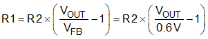
To keep the feedback (FB) net robust from noise, set R2 equal to or lower than 100 kΩ to have at least 6 µA of current in the voltage divider. Lower values of FB resistors achieve better noise immunity but lower light-load efficiency, as explained in the Design Considerations for a Resistive Feedback Divider in a DC/DC Converter Technical Brief.

When a fixed output voltage is selected, connect the FB pin directly to the output. R1 and R2 are not needed, as VOUT is set through a resistor on the VSET/MODE pin. Select the recommended resistor value from the list in Table 7-2.