SLVSHR7 August   2024 TPSM8287A12M , TPSM8287A15M

PRODUCTION DATA  

  1.   1
  2. Features
  3. Applications
  4. Description
  5. Device Options
  6. Pin Configuration and Functions
  7. Specifications
    1. 6.1 Absolute Maximum Ratings
    2. 6.2 ESD Ratings
    3. 6.3 Recommended Operating Conditions
    4. 6.4 Thermal Information
    5. 6.5 Electrical Characteristics
    6. 6.6 I2C Interface Timing Characteristics
    7. 6.7 Typical Characteristics
  8. Detailed Description
    1. 7.1 Overview
    2. 7.2 Functional Block Diagram
    3. 7.3 Feature Description
      1. 7.3.1  Fixed-Frequency DCS-Control Topology
      2. 7.3.2  Forced-PWM and Power Save Modes
      3. 7.3.3  Precise Enable
      4. 7.3.4  Start-Up
      5. 7.3.5  Switching Frequency Selection
      6. 7.3.6  Output Voltage Setting
        1. 7.3.6.1 Output Voltage Setpoint
        2. 7.3.6.2 Output Voltage Range
        3. 7.3.6.3 Non-Default Output Voltage Setpoint
        4. 7.3.6.4 Dynamic Voltage Scaling (DVS)
      7. 7.3.7  Compensation (COMP)
      8. 7.3.8  Mode Selection / Clock Synchronization (MODE/SYNC)
      9. 7.3.9  Spread Spectrum Clocking (SSC)
      10. 7.3.10 Output Discharge
      11. 7.3.11 Undervoltage Lockout (UVLO)
      12. 7.3.12 Overvoltage Lockout (OVLO)
      13. 7.3.13 Overcurrent Protection
        1. 7.3.13.1 Cycle-by-Cycle Current Limiting
        2. 7.3.13.2 Hiccup Mode
        3. 7.3.13.3 Current-Limit Mode
      14. 7.3.14 Power Good (PG)
        1. 7.3.14.1 Power-Good Standalone, Primary Device Behavior
        2. 7.3.14.2 Power-Good Secondary Device Behavior
      15. 7.3.15 Remote Sense
      16. 7.3.16 Thermal Warning and Shutdown
      17. 7.3.17 Stacked Operation
    4. 7.4 Device Functional Modes
      1. 7.4.1 Power-On Reset (POR)
      2. 7.4.2 Undervoltage Lockout
      3. 7.4.3 Standby
      4. 7.4.4 On
    5. 7.5 Programming
      1. 7.5.1 Serial Interface Description
      2. 7.5.2 Standard-, Fast-, Fast-Mode Plus Protocol
      3. 7.5.3 I2C Update Sequence
      4. 7.5.4 I2C Register Reset
  9. Device Registers
  10. Application and Implementation
    1. 9.1 Application Information
    2. 9.2 Typical Application
      1. 9.2.1 Design Requirements
      2. 9.2.2 Detailed Design Procedure
        1. 9.2.2.1 Selecting the Input Capacitors
        2. 9.2.2.2 Selecting the Target Loop Bandwidth
        3. 9.2.2.3 Selecting the Compensation Resistor
        4. 9.2.2.4 Selecting the Output Capacitors
        5. 9.2.2.5 Selecting the Compensation Capacitor, CComp1
        6. 9.2.2.6 Selecting the Compensation Capacitor, CComp2
      3. 9.2.3 Application Curves
    3. 9.3 Typical Application Using Four TPSM8287A1xM in Parallel Operation
      1. 9.3.1 Design Requirements
      2. 9.3.2 Detailed Design Procedure
        1. 9.3.2.1 Selecting the Input Capacitors
        2. 9.3.2.2 Selecting the Target Loop Bandwidth
        3. 9.3.2.3 Selecting the Compensation Resistor
        4. 9.3.2.4 Selecting the Output Capacitors
        5. 9.3.2.5 Selecting the Compensation Capacitor, CComp1
        6. 9.3.2.6 Selecting the Compensation Capacitor, CComp2
      3. 9.3.3 Application Curves
    4. 9.4 Power Supply Recommendations
    5. 9.5 Layout
      1. 9.5.1 Layout Guidelines
      2. 9.5.2 Layout Example
  11. 10Device and Documentation Support
    1. 10.1 Device Support
      1. 10.1.1 Third-Party Products Disclaimer
    2. 10.2 Documentation Support
      1. 10.2.1 Related Documentation
    3. 10.3 Receiving Notification of Documentation Updates
    4. 10.4 Support Resources
    5. 10.5 Trademarks
    6. 10.6 Electrostatic Discharge Caution
    7. 10.7 Glossary
  12. 11Revision History
  13. 12Mechanical, Packaging, and Orderable Information
    1. 12.1 Tape and Reel Information

Package Options

Mechanical Data (Package|Pins)
Thermal pad, mechanical data (Package|Pins)
Orderable Information

Hiccup Mode

Hiccup mode reduces the power dissipation during an overload event. To enable hiccup operation, make sure that HICCUPEN  = 1 in the CONTROL1 register. If hiccup operation is enabled and the high-side switch current hits the high-side current limit threshold on 32 consecutive switching cycles, the device:

  • Stops switching for 128µs, after which the device automatically starts switching again (the device starts a new soft-start sequence)
  • Sets the HICCUP bit in the STATUS register
  • Pulls the PG pin low. The PG pin stays low until the overload condition goes away and the device can start up and regulate the output voltage.

Hiccup operation continues – in a repeating sequence of 32 cycles in current limit, followed by a pause of 128µs, followed by a soft-start attempt – for as long as the output overload condition exists.

The device clears the HICCUP bit if reading the STATUS register when the overload condition no longer exists. Figure 7-18 shows 2 cycles of hiccup operation, at which point the over load is removed and the part continues in normal operation.
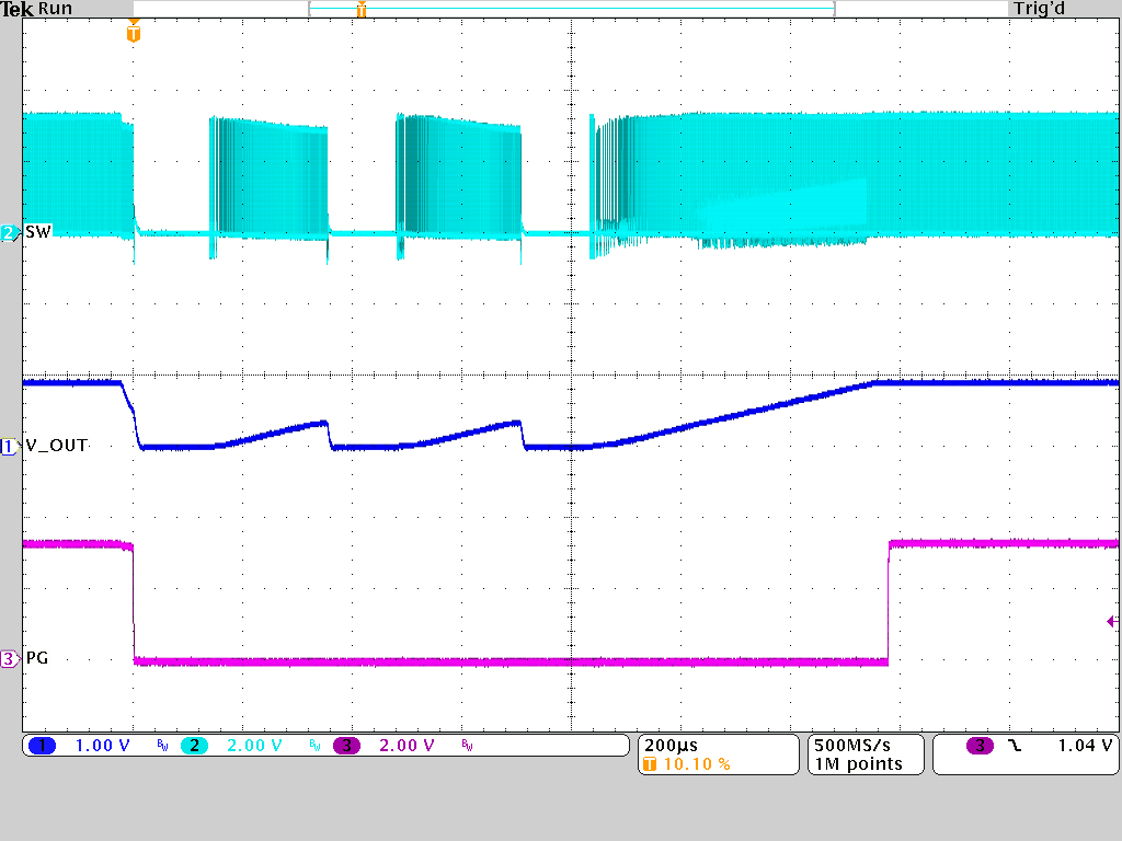

TPSM8287A12M TPSM8287A15M Hiccup Current Limit
Figure 7-18 Hiccup Current Limit