SLVSG68 November 2022 TPSM82901
PRODUCTION DATA
- 1 Features
- 2 Applications
- 3 Description
- 4 Revision History
- 5 Pin Configuration and Functions
- 6 Specifications
-
7 Detailed Description
- 7.1 Overview
- 7.2 Functional Block Diagram
- 7.3
Feature Description
- 7.3.1 Mode Selection and Device Configuration (MODE/S-CONF)
- 7.3.2 Adjustable VO Operation (External Voltage Divider)
- 7.3.3 Setable VO Operation (VSET and Internal Voltage Divider)
- 7.3.4 Soft Start/Tracking (SS/TR)
- 7.3.5 Smart Enable with Precise Threshold
- 7.3.6 Power Good (PG)
- 7.3.7 Undervoltage Lockout (UVLO)
- 7.3.8 Current Limit And Short Circuit Protection
- 7.3.9 Thermal Shutdown
- 7.4 Device Functional Modes
- 8 Application and Implementation
- 9 Device and Documentation Support
- 10Mechanical, Packaging, and Orderable Information
Package Options
Mechanical Data (Package|Pins)
- SIS|11
Thermal pad, mechanical data (Package|Pins)
Orderable Information
7.3.3 Setable VO Operation (VSET and Internal Voltage Divider)
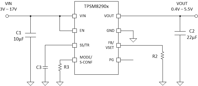
If the device is configured to VSET operation, VO is sensed only through the internal VOS connection by an internal resistor divider. The target VO is programmed by an external resistor connected between the VSET pin and GND. Figure 7-3 shows the typical schematic for this configuration.
 Figure 7-3 Setable VO
Operation Schematic
Figure 7-3 Setable VO
Operation SchematicTable 7-3 VSET Selection Table
| # | Resistor Value [Ω] | Target VO [V] |
|---|---|---|
| 1 | GND | 1.2 |
| 2 | 4.64 k | 0.4 |
| 3 | 5.76 k | 0.6 |
| 4 | 7.15 k | 0.8 |
| 5 | 8.87 k | 1.0 |
| 6 | 11.0 k | 1.1 |
| 7 | 13.7 k | 1.3 |
| 8 | 16.9 k | 1.35 |
| 9 | 21.0 k | 1.8 |
| 10 | 26.1 k | 1.9 |
| 11 | 40.2 k | 2.5 |
| 12 | 61.9 k | 3.8 |
| 13 | 76.8 k | 5.0 |
| 14 | 95.3 k | 5.1 |
| 15 | 118.0 k | 5.5 |
| 16 | 249.00 k or larger/Open | 3.3 |