SLUSCV7A July 2017 – August 2017 TPSM84203 , TPSM84205 , TPSM84212
PRODUCTION DATA.
- 1 Features
- 2 Applications
- 3 Description
- 4 Revision History
- 5 Pin Configuration and Functions
- 6 Specifications
- 7 Detailed Description
- 8 Application and Implementation
- 9 Power Supply Recommendations
- 10Layout
- 11Device and Documentation Support
- 12Mechanical, Packaging, and Orderable Information
Package Options
Mechanical Data (Package|Pins)
- EAB|3
Thermal pad, mechanical data (Package|Pins)
Orderable Information
10 Layout
10.1 Layout Guidelines
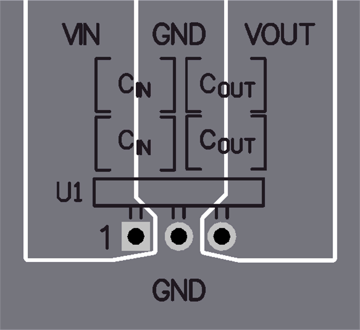
To achieve optimal electrical and thermal performance, an optimized PCB layout is required. Figure 28 shows a typical PCB layout. Some considerations for an optimized layout are:
- Use large copper areas for power planes (VIN, VOUT, and GND) to minimize conduction loss and thermal stress.
- Place ceramic input and output capacitors close to the device pins to minimize high frequency noise.
- Locate additional output capacitors between the ceramic capacitor and the load.
- Use multiple vias to connect the power planes to internal layers.
10.2 Layout Example
 Figure 28.