SLVSE31C January 2018 – July 2018 TPSM84209
PRODUCTION DATA.
- 1 Features
- 2 Applications
- 3 Description
- 4 Revision History
- 5 Pin Configuration and Functions
- 6 Specifications
-
7 Detailed Description
- 7.1 Overview
- 7.2 Functional Block Diagram
- 7.3
Feature Description
- 7.3.1 Adjusting the Output Voltage
- 7.3.2 Input Capacitor Selection
- 7.3.3 Undervoltage Lockout (UVLO)
- 7.3.4 Output Capacitor Selection
- 7.3.5 Feed-Forward Capacitor
- 7.3.6 Operating Range
- 7.3.7 Output Current Rating
- 7.3.8 Enable (EN)
- 7.3.9 Internal Soft Start
- 7.3.10 Safe Start-Up Into Prebiased Outputs
- 7.3.11 Light Load Efficiency / Eco-Mode
- 7.3.12 Voltage Dropout
- 7.3.13 Overcurrent Protection
- 7.3.14 Output Overvoltage Protection (OVP)
- 7.3.15 Thermal Performance
- 7.3.16 Thermal Shutdown
- 7.4 Device Functional Modes
- 8 Application and Implementation
- 9 Power Supply Recommendations
- 10Layout
- 11Device and Documentation Support
- 12Mechanical, Packaging, and Orderable Information
Package Options
Refer to the PDF data sheet for device specific package drawings
Mechanical Data (Package|Pins)
- RKH|9
Thermal pad, mechanical data (Package|Pins)
Orderable Information
7.3.8 Enable (EN)
The EN pin provides electrical ON and OFF control of the device. When the EN pin voltage exceeds the threshold voltage, the device begins operation. If the EN pin voltage is pulled below the threshold voltage, the regulator stops switching and enters the low-quiescent current state.
The EN pin has an internal pullup-current source, which allows the user to float the EN pin to enable the device. If an application requires control of the EN pin, use open-drain or open-collector output logic to interface with the pin.
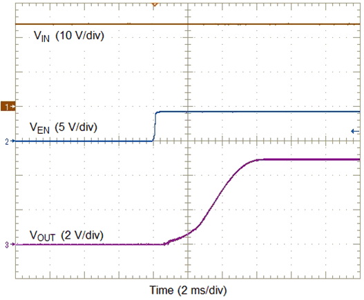
Figure 23 shows the typical application of the enable function. Turning Q1 on applies a low voltage to the enable control pin and disables the output of the supply, shown in Figure 24. If Q1 is turned off, the supply executes a soft-start power-up sequence, as shown in Figure 25.
 Figure 23. Typical Enable Control
  Figure 24. Enable Turnoff
  Figure 25. Enable Turnon