SLUSFH2 January 2024 TPSM843320E
PRODUCTION DATA
- 1
- 1 Features
- 2 Applications
- 3 Description
- 4 Pin Configuration and Functions
- 5 Specifications
-
6 Detailed Description
- 6.1 Overview
- 6.2 Functional Block Diagram
- 6.3
Feature Description
- 6.3.1 VIN Pins and VIN UVLO
- 6.3.2 Enable and Adjustable UVLO
- 6.3.3 Adjusting the Output Voltage
- 6.3.4 Switching Frequency Selection
- 6.3.5 Switching Frequency Synchronization to an External Clock
- 6.3.6 Ramp Amplitude Selection
- 6.3.7 Soft Start and Prebiased Output Start-Up
- 6.3.8 Mode Pin
- 6.3.9 Power Good (PGOOD)
- 6.3.10 Current Protection
- 6.3.11 Output Overvoltage and Undervoltage Protection
- 6.3.12 Overtemperature Protection
- 6.3.13 Output Voltage Discharge
- 6.4 Device Functional Modes
-
7 Application and Implementation
- 7.1 Application Information
- 7.2
Typical Applications
- 7.2.1
1.0V Output, 1MHz
Application
- 7.2.1.1 Design Requirements
- 7.2.1.2
Detailed Design Procedure
- 7.2.1.2.1 Switching Frequency
- 7.2.1.2.2 Output Inductor Selection
- 7.2.1.2.3 Output Capacitor
- 7.2.1.2.4 Input Capacitor
- 7.2.1.2.5 Adjustable Undervoltage Lockout
- 7.2.1.2.6 Output Voltage Resistors Selection
- 7.2.1.2.7 Bootstrap Capacitor Selection
- 7.2.1.2.8 BP5 Capacitor Selection
- 7.2.1.2.9 PGOOD Pullup Resistor
- 7.2.1.2.10 Current Limit Selection
- 7.2.1.2.11 Soft-Start Time Selection
- 7.2.1.2.12 Ramp Selection and Control Loop Stability
- 7.2.1.2.13 MODE Pin
- 7.2.1.3 Application Curves
- 7.2.1
1.0V Output, 1MHz
Application
- 7.3 Power Supply Recommendations
- 7.4 Layout
- 8 Device and Documentation Support
- 9 Revision History
- 10Mechanical, Packaging, and Orderable Information
Package Options
Mechanical Data (Package|Pins)
- SIT|15
Thermal pad, mechanical data (Package|Pins)
Orderable Information
6.3.5.2 Loss of Synchronization
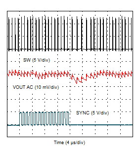
If at any time during operation, there is a loss of synchronization, the device defaults to the internal PWM oscillator frequency until the synchronization clock returns. After the clock is no longer present, the device switches at 70% of the internal clock frequency for four consecutive cycles. After four consecutive cycles without clock pulses, the device operates at the normal internal PWM oscillator frequency. This action is demonstrated in Figure 6-4.
 Figure 6-4 Clock Synchronization Transitions