SLUSFH2 January 2024 TPSM843320E
PRODUCTION DATA
- 1
- 1 Features
- 2 Applications
- 3 Description
- 4 Pin Configuration and Functions
- 5 Specifications
-
6 Detailed Description
- 6.1 Overview
- 6.2 Functional Block Diagram
- 6.3
Feature Description
- 6.3.1 VIN Pins and VIN UVLO
- 6.3.2 Enable and Adjustable UVLO
- 6.3.3 Adjusting the Output Voltage
- 6.3.4 Switching Frequency Selection
- 6.3.5 Switching Frequency Synchronization to an External Clock
- 6.3.6 Ramp Amplitude Selection
- 6.3.7 Soft Start and Prebiased Output Start-Up
- 6.3.8 Mode Pin
- 6.3.9 Power Good (PGOOD)
- 6.3.10 Current Protection
- 6.3.11 Output Overvoltage and Undervoltage Protection
- 6.3.12 Overtemperature Protection
- 6.3.13 Output Voltage Discharge
- 6.4 Device Functional Modes
-
7 Application and Implementation
- 7.1 Application Information
- 7.2
Typical Applications
- 7.2.1
1.0V Output, 1MHz
Application
- 7.2.1.1 Design Requirements
- 7.2.1.2
Detailed Design Procedure
- 7.2.1.2.1 Switching Frequency
- 7.2.1.2.2 Output Inductor Selection
- 7.2.1.2.3 Output Capacitor
- 7.2.1.2.4 Input Capacitor
- 7.2.1.2.5 Adjustable Undervoltage Lockout
- 7.2.1.2.6 Output Voltage Resistors Selection
- 7.2.1.2.7 Bootstrap Capacitor Selection
- 7.2.1.2.8 BP5 Capacitor Selection
- 7.2.1.2.9 PGOOD Pullup Resistor
- 7.2.1.2.10 Current Limit Selection
- 7.2.1.2.11 Soft-Start Time Selection
- 7.2.1.2.12 Ramp Selection and Control Loop Stability
- 7.2.1.2.13 MODE Pin
- 7.2.1.3 Application Curves
- 7.2.1
1.0V Output, 1MHz
Application
- 7.3 Power Supply Recommendations
- 7.4 Layout
- 8 Device and Documentation Support
- 9 Revision History
- 10Mechanical, Packaging, and Orderable Information
Package Options
Mechanical Data (Package|Pins)
- SIT|15
Thermal pad, mechanical data (Package|Pins)
Orderable Information
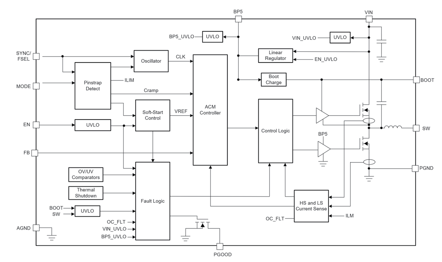
6.2 Functional Block Diagram
