SLVSE06B January   2018  – JANUARY 2019 TPSM846C24

PRODUCTION DATA.  

  1. Features
  2. Applications
  3. Description
    1.     Device Images
      1.      Simplified Schematic
      2.      Efficiency vs Output Current
  4. Revision History
  5. Pin Configuration and Functions
    1.     Pin Functions
  6. Specifications
    1. 6.1 Absolute Maximum Ratings
    2. 6.2 ESD Ratings
    3. 6.3 Recommended Operating Conditions
    4. 6.4 Thermal Information
    5. 6.5 Electrical Characteristics
    6. 6.6 Switching Characteristics
    7. 6.7 Typical Characteristics (VIN = 12 V)
    8. 6.8 Typical Characteristics (VIN = 5 V)
  7. Detailed Description
    1. 7.1 Overview
    2. 7.2 Functional Block Diagram
    3. 7.3 Feature Description
      1. 7.3.1  Minimum Capacitance Requirements
      2. 7.3.2  Setting the Compensation Network
      3. 7.3.3  Transient Response
      4. 7.3.4  Setting the Output Voltage
      5. 7.3.5  Differential Remote Sense
      6. 7.3.6  Switching Frequency and Synchronization
        1. 7.3.6.1 Setting the Switching Frequency
        2. 7.3.6.2 Synchronization
          1. 7.3.6.2.1 Stand-Alone Device Synchronization
          2. 7.3.6.2.2 Paralleled Devices Synchronization
      7. 7.3.7  Prebiased Output Start-Up
      8. 7.3.8  Power-Good (PGOOD) Indicator
      9. 7.3.9  Linear Regulators BP3 and BP6
      10. 7.3.10 Parallel Application
      11. 7.3.11 Parallel Operation
      12. 7.3.12 Overtemperature Protection
      13. 7.3.13 Overcurrent Protection
      14. 7.3.14 Output Overvoltage and Undervoltage Protection
    4. 7.4 Device Functional Modes
      1. 7.4.1 Active Mode
      2. 7.4.2 Shutdown Mode
  8. Application and Implementation
    1. 8.1 Typical Application
      1. 8.1.1 Design Requirements
      2. 8.1.2 Detailed Design Procedure
        1. 8.1.2.1 Custom Design With WEBENCH® Tools
        2. 8.1.2.2 Setting the Output Voltage
        3. 8.1.2.3 Input and Output Capacitance
        4. 8.1.2.4 Selecting the Compensation Components
        5. 8.1.2.5 Setting the Switching Frequency
        6. 8.1.2.6 Power Good (PGOOD)
        7. 8.1.2.7 ON/OFF Control (EN)
      3. 8.1.3 Application Curves
  9. Power Supply Recommendations
  10. 10Layout
    1. 10.1 Layout Guidelines
    2. 10.2 Layout Example
    3. 10.3 Package Specifications
    4. 10.4 EMI
    5. 10.5 Mounting and Thermal Profile Recommendation
  11. 11Device and Documentation Support
    1. 11.1 Device Support
      1. 11.1.1 Development Support
        1. 11.1.1.1 Custom Design With WEBENCH® Tools
    2. 11.2 Receiving Notification of Documentation Updates
    3. 11.3 Community Resources
    4. 11.4 Trademarks
    5. 11.5 Electrostatic Discharge Caution
    6. 11.6 Glossary
  12. 12Mechanical, Packaging, and Orderable Information
    1. 12.1 Tape and Reel Information

Package Options

Mechanical Data (Package|Pins)
Thermal pad, mechanical data (Package|Pins)
Orderable Information

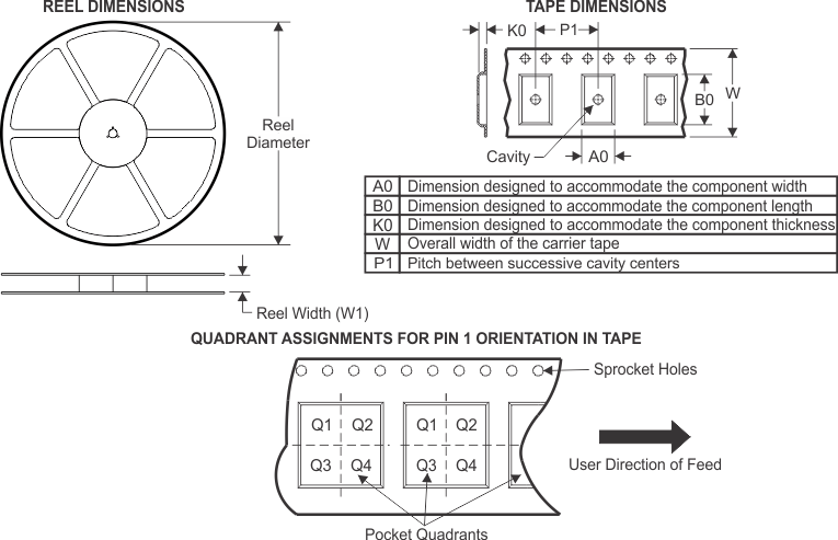
Tape and Reel Information

TPSM846C24 Tape_and_Reel_Dims.gif
Device Package
Type
Package Drawing Pins SPQ Reel
Diameter (mm)
Reel
Width W1 (mm)
A0
(mm)
B0
(mm)
K0
(mm)
P1
(mm)
W
(mm)
Pin1
Quadrant
TPSM846C24MOLR QFM MOL 59 350 330.0 32.4 15.35 16.35 6.1 24.0 32.0 Q1

TPSM846C24 Tape_and_Reel_Box_Dims.gif

Device Package Type Package Drawing Pins SPQ Length (mm) Width (mm) Height (mm)
TPSM846C24MOLR QFM MOL 59 350 383.0 353.0 58.0