SLVSDF7A December 2016 – July 2017 TPSM84A21
PRODUCTION DATA.
- 1 Features
- 2 Applications
- 3 Description
- 4 Revision History
- 5 Pin Configuration and Functions
- 6 Specifications
-
7 Detailed Description
- 7.1 Overview
- 7.2 Functional Block Diagram
- 7.3
Feature Description
- 7.3.1 Adjusting the Output Voltage (VADJ)
- 7.3.2 Input and Output Capacitance
- 7.3.3 Transient Response
- 7.3.4 Oscillator Frequency
- 7.3.5 External Clock Syncronization
- 7.3.6 Soft Start
- 7.3.7 Power Good (PGOOD)
- 7.3.8 Gate Driver (VG)
- 7.3.9 Startup into Pre-biased Outputs
- 7.3.10 Thermal Shutdown
- 7.3.11 Overcurrent Protection
- 7.3.12 Output Undervoltage/Overvoltage Protection
- 7.3.13 Enable (EN)
- 7.3.14 Undervoltage Lockout (UVLO)
- 7.4 Device Functional Modes
- 8 Application and Implementation
- 9 Power Supply Recommendations
- 10Layout
- 11Device and Documentation Support
- 12Mechanical, Packaging, and Orderable Information
Package Options
Mechanical Data (Package|Pins)
- MOJ|20
Thermal pad, mechanical data (Package|Pins)
Orderable Information
6.8 Typical Characteristics
The electrical characteristic data has been developed from actual products tested at 25°C. This data is considered typical for the converter. Applies to Figure 1 through Figure 4.
The temperature derating curves represent the conditions at which internal components are at or below the manufacturer's maximum operating temperatures. Derating limits apply to devices soldered directly to a 50 mm × 100 mm double-sided PCB with 2 oz. copper. Applies to Figure 5 and Figure 6.
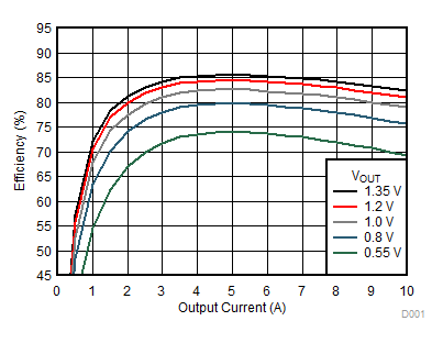
| VIN = 12 V | VG = open |
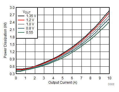
| VIN = 12 V | VG = open |
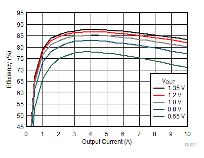
| VIN = 12 V | VG = 5 V |
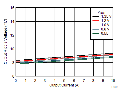
| VIN = 12 V |
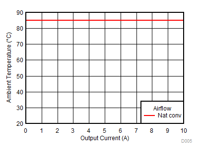
| VIN = 12 V | VOUT = 0.8 V |
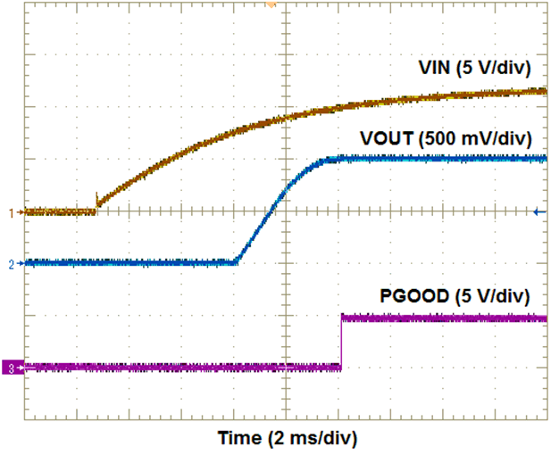
1.
Figure 7. VIN Start-up Waveforms | VIN = 12 V | VOUT = 1.0 V | IOUT = 1 A |
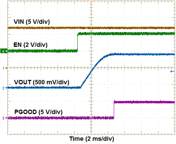
1.
Figure 9. EN Start-up Waveforms | VIN = 12 V | VOUT = 1.0 V | IOUT = 1 A |
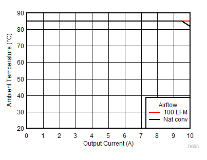
| VIN = 12 V | VOUT = 1.2 V |
1.
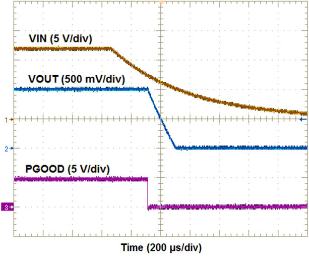
Figure 8. VIN Shut-down Waveforms | VIN = 12 V | VOUT = 1.0 V | IOUT = 1 A |
1.
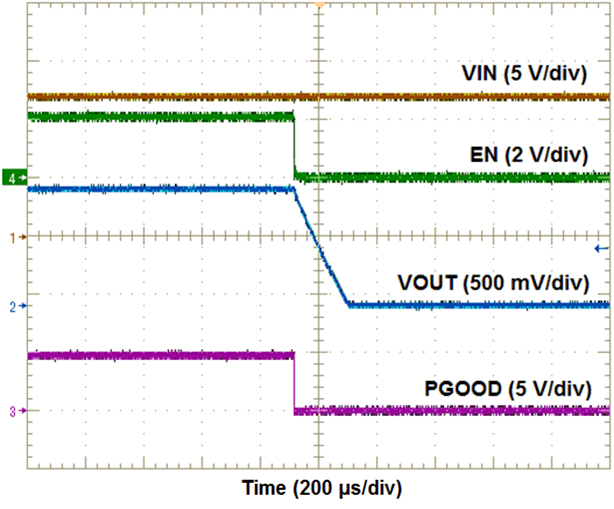
Figure 10. EN Shut-down Waveforms | VIN = 12 V | VOUT = 1.0 V | IOUT = 1 A |