SLVSDF8B December   2016  – July 2017 TPSM84A22

PRODUCTION DATA.  

  1. Features
  2. Applications
  3. Description
    1.     Device Images
      1.      Simplified Schematic
      2.      Transient Response
  4. Revision History
  5. Pin Configuration and Functions
    1.     Pin Functions
  6. Specifications
    1. 6.1 Absolute Maximum Ratings
    2. 6.2 ESD Ratings
    3. 6.3 Recommended Operating Conditions
    4. 6.4 Thermal Information
    5. 6.5 Electrical Characteristics
    6. 6.6 Switching Characteristics
    7. 6.7 Package Specifications
    8. 6.8 Typical Characteristics
  7. Detailed Description
    1. 7.1 Overview
    2. 7.2 Functional Block Diagram
    3. 7.3 Feature Description
      1. 7.3.1  Adjusting the Output Voltage (VADJ)
      2. 7.3.2  Input and Output Capacitance
      3. 7.3.3  Transient Response
        1. 7.3.3.1 Transient Response Waveforms
      4. 7.3.4  Oscillator Frequency
      5. 7.3.5  External Clock Syncronization
      6. 7.3.6  Soft Start
      7. 7.3.7  Power Good (PGOOD)
      8. 7.3.8  Gate Driver (VG)
      9. 7.3.9  Startup into Pre-biased Outputs
      10. 7.3.10 Thermal Shutdown
      11. 7.3.11 Overcurrent Protection
      12. 7.3.12 Output Undervoltage/Overvoltage Protection
      13. 7.3.13 Enable (EN)
      14. 7.3.14 Undervoltage Lockout (UVLO)
    4. 7.4 Device Functional Modes
      1. 7.4.1 Active Mode
      2. 7.4.2 Light Load Operation
      3. 7.4.3 Shutdown Mode
  8. Application and Implementation
    1. 8.1 Application Information
    2. 8.2 Typical Application
      1. 8.2.1 Design Requirements
      2. 8.2.2 Detailed Design Procedure
        1. 8.2.2.1 Setting the Output Voltage
        2. 8.2.2.2 Input and Output Capacitance
        3. 8.2.2.3 Power Good (PGOOD)
        4. 8.2.2.4 External VG Voltage
      3. 8.2.3 Application Curves
  9. Power Supply Recommendations
  10. 10Layout
    1. 10.1 Layout Guidelines
    2. 10.2 Layout Examples
    3. 10.3 EMI
  11. 11Device and Documentation Support
    1. 11.1 Documentation Support
      1. 11.1.1 Related Documentation
    2. 11.2 Receiving Notification of Documentation Updates
    3. 11.3 Community Resources
    4. 11.4 Trademarks
    5. 11.5 Electrostatic Discharge Caution
    6. 11.6 Glossary
  12. 12Mechanical, Packaging, and Orderable Information
    1. 12.1 Tape and Reel Information

Package Options

Mechanical Data (Package|Pins)
Thermal pad, mechanical data (Package|Pins)
Orderable Information

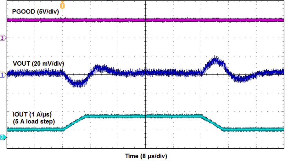
Transient Response Waveforms

TPSM84A22 Trans1_2_1A.gif
VIN = 12V VOUT = 1.2 V Load Step = 5 A
COUT = 0 µF Slew Rate = 1 A/µs
Figure 12. Transient Response
TPSM84A22 Trans1_8_1A.gif
VIN = 12V VOUT = 1.8 V Load Step = 5 A
COUT = 0 µF Slew Rate = 1 A/µs
Figure 14. Transient Response
TPSM84A22 Trans1_2_5A.gif
VIN = 12V VOUT = 1.2 V Load Step = 5 A
COUT = 0 µF Slew Rate = 5 A/µs
Figure 13. Transient Response
TPSM84A22 Trans1_8_5A.gif
VIN = 12V VOUT = 1.8 V Load Step = 5 A
COUT = 0 µF Slew Rate = 5 A/µs
Figure 15. Transient Response