SBOS972C october   2021  – august 2023 TRF1208

PRODUCTION DATA  

  1.   1
  2. Features
  3. Applications
  4. Description
  5. Revision History
  6. Pin Configuration and Functions
  7. Specifications
    1. 6.1 Absolute Maximum Ratings
    2. 6.2 ESD Ratings
    3. 6.3 Recommended Operating Conditions
    4. 6.4 Thermal Information
    5. 6.5 Electrical Characteristics: TRF1208
    6. 6.6 Electrical Characteristics: TRF1208B
    7. 6.7 Typical Characteristics: TRF1208
    8. 6.8 Typical Characteristics: TRF1208B
  8. Detailed Description
    1. 7.1 Overview
    2. 7.2 Functional Block Diagram
    3. 7.3 Feature Description
      1. 7.3.1 Fully-Differential Amplifier
      2. 7.3.2 Single Supply Operation
    4. 7.4 Device Functional Modes
      1. 7.4.1 Power-Down Mode
  9. Application and Implementation
    1. 8.1 Application Information
      1. 8.1.1 Driving a High-Speed ADC
      2. 8.1.2 Calculating Output Voltage Swing
      3. 8.1.3 Thermal Considerations
    2. 8.2 Typical Applications
      1. 8.2.1 TRF1208 in Receive Chain
        1. 8.2.1.1 Design Requirements
        2. 8.2.1.2 Detailed Design Procedure
      2. 8.2.2 TRF1208 in a Transmit Chain
        1. 8.2.2.1 Design Requirements
        2. 8.2.2.2 Detailed Design Procedure
    3. 8.3 Power Supply Recommendations
    4. 8.4 Layout
      1. 8.4.1 Layout Guidelines
      2. 8.4.2 Layout Example
  10. Device and Documentation Support
    1. 9.1 Device Support
      1. 9.1.1 Third-Party Products Disclaimer
    2. 9.2 Documentation Support
      1. 9.2.1 Related Documentation
    3. 9.3 Receiving Notification of Documentation Updates
    4. 9.4 Support Resources
    5. 9.5 Trademarks
    6. 9.6 Electrostatic Discharge Caution
    7. 9.7 Glossary
  11. 10Mechanical, Packaging, and Orderable Information

Package Options

Mechanical Data (Package|Pins)
Thermal pad, mechanical data (Package|Pins)
Orderable Information

Typical Characteristics: TRF1208

at temperature = 25°C, VDD = 3.3 V, 50-Ω single-ended input, and 100-Ω differential output (unless otherwise noted)

GUID-20210830-SS0I-HMDP-9ZCH-H0TPSSPGM3H2-low.gif
Figure 6-1 Power Gain Across Temperature
GUID-20210830-SS0I-BJGR-FHR1-DBV000NL3CTK-low.gif
Figure 6-3 Return Loss Across Temperature
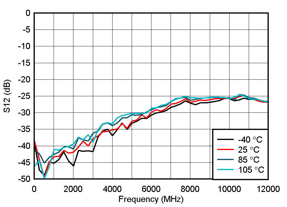
GUID-20210830-SS0I-K90P-N8TQ-CT56RH8LGPZQ-low.gif
Figure 6-5 Reverse Isolation Across Temperature
GUID-20210830-SS0I-XXS2-C2CD-GXR5TDKPQNVR-low.gif
Pout /tone = -4 dBm, 10 MHz tone spacing
Figure 6-7 OIP3 Across Temperature
GUID-20210830-SS0I-CQVR-92PW-MVCFDPQWZ65J-low.gif
At (2f1-f2) frequency, f1 < f2; Pout /tone = -4 dBm, 10 MHz tone spacing
Figure 6-9 IMD3 Lower Across Temperature
GUID-20210830-SS0I-FBJG-KZKF-R6NZLVM2RKMH-low.gif
At (2f2-f1) frequency, f1 < f2; Pout /tone = -4 dBm, 10 MHz tone spacing
Figure 6-11 IMD3 Higher Across Temperature
GUID-20210830-SS0I-WKLB-7MRM-LSZC0V1NKXFR-low.gif
At (f2-f1) frequency, f2 > f1; Pout /tone = -4 dBm, 10 MHz tone spacing
Figure 6-13 OIP2 Lower Across Temperature
GUID-20210830-SS0I-7FKG-GGBR-3ZRVD68KM1KM-low.gif
At (f2+f1) frequency, f2 > f1; Pout /tone = -4 dBm, 10 MHz tone spacing
Figure 6-15 OIP2 Higher Across Temperature
GUID-20210830-SS0I-DLTW-CNH7-CJWJZTXGZKTZ-low.gif
At (f2-f1) frequency, f2 > f1; Pout /tone = -4 dBm, 10 MHz tone spacing
Figure 6-17 IMD2 Lower Across Temperature
GUID-20210830-SS0I-BM0T-LHRZ-T3JZLG4GJCRB-low.gif
At (f2+f1) frequency, f2 > f1; Pout /tone = -4 dBm, 10 MHz tone spacing
Figure 6-19 IMD2 Higher Across Temperature
GUID-20210830-SS0I-PMN0-8HHT-FQ8PLDD9WMQS-low.gif
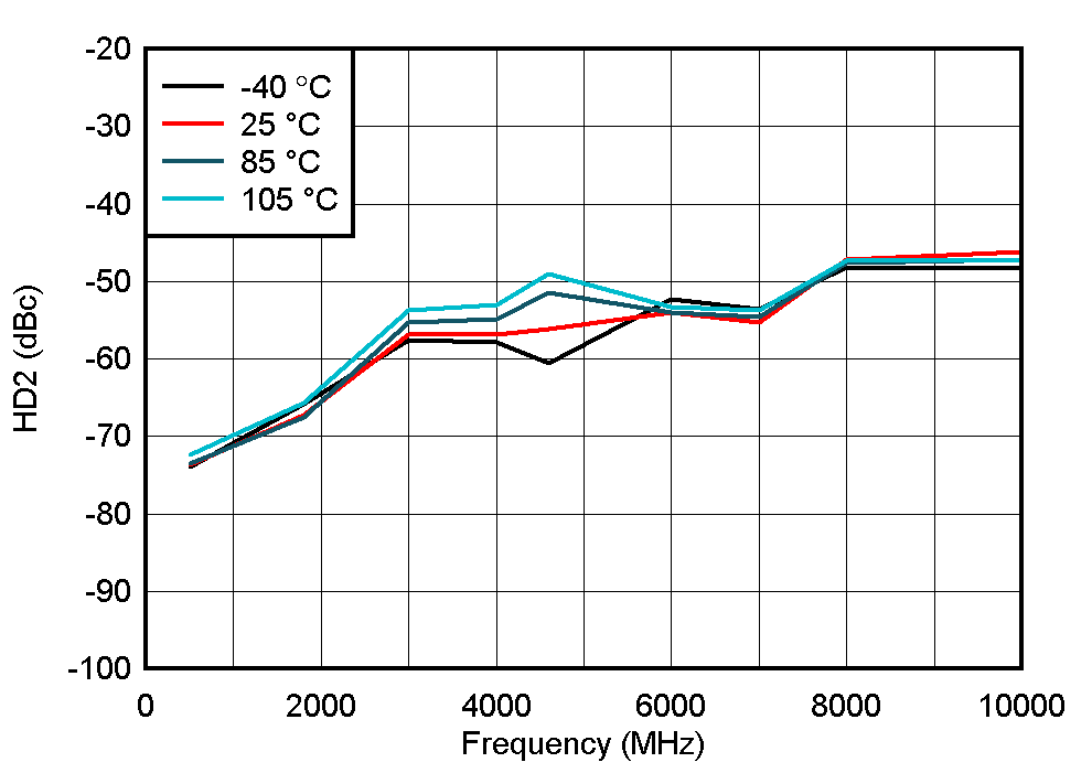
Pout = +3 dBm
Figure 6-21 HD2 Across Temperature
GUID-20210830-SS0I-HJVR-ZGR5-MH7VF7CJCJTF-low.gif
Pout = +3 dBm
Figure 6-23 HD3 Across Temperature
GUID-20210830-SS0I-NSVQ-CW20-2NS0SZQ7QXTW-low.svg
Figure 6-25 HD2 vs Output Power
GUID-20210830-SS0I-LBT3-7HBK-SJBP01BJKXQQ-low.gif
Figure 6-27 Output P1dB Across Temperature
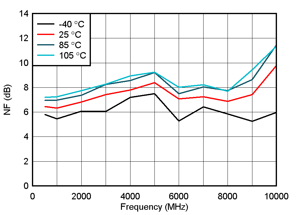
GUID-20210830-SS0I-LG8T-TKZ9-Z9MCQ2M0BKSQ-low.gif
Figure 6-29 NF Across Temperature
GUID-20210830-SS0I-FT0D-DJNH-RJZTDMCT2RNJ-low.gif
Figure 6-31 Gain Imbalance
GUID-20210830-SS0I-JCRP-67SR-XGLWMTVQGNXL-low.gif
Figure 6-33 CMRR Across Temperature
GUID-20210922-SS0I-QHKN-KQJJ-ZHJCQHGSRW8S-low.svg
Input = -2 dBm, f = 500 MHz
Figure 6-35 Overdrive Recovery
GUID-20210923-SS0I-JMTW-HLBB-DDNHRWFGK1GL-low.svg
Figure 6-37 Single-Ended S11
GUID-20210830-SS0I-GFG2-DV0T-D2TRQ5FNK5MN-low.svg
Figure 6-2 Power Gain Across VDD
GUID-20210830-SS0I-6FMS-VRXX-XPD9BLMZW0ZN-low.svg
Figure 6-4 Return Loss Across VDD
GUID-20210830-SS0I-KQS1-SSJH-T6QMGRSVLXC3-low.svg
Figure 6-6 Reverse Isolation Across VDD
GUID-20210830-SS0I-KWFN-0MTV-QFW4TNSTDGSS-low.svg
Pout /tone = -4 dBm, 10 MHz tone spacing
Figure 6-8 OIP3 Across VDD
GUID-20210830-SS0I-2TJK-KSW4-CBXV8NJJPGRL-low.svg
At (2f1-f2) frequency, f1 < f2; Pout /tone = -4 dBm, 10 MHz tone spacing
Figure 6-10 IMD3 Lower Across VDD
GUID-20210830-SS0I-1CQP-F2QW-GJQ5N9RKGWDC-low.svg
At (2f2-f1) frequency, f1 < f2; Pout /tone = -4 dBm, 10 MHz tone spacing
Figure 6-12 IMD3 Higher Across VDD
GUID-20210830-SS0I-JDKN-GQPZ-84MKMK35B9W3-low.svg
At (f2-f1) frequency, f2 > f1; Pout /tone = -4 dBm, 10 MHz tone spacing
Figure 6-14 OIP2 Lower Across VDD
GUID-20210830-SS0I-RB4N-ZNPX-X4HKD7PC2RTG-low.svg
At (f2+f1) frequency, f2 > f1; Pout /tone = -4 dBm, 10 MHz tone spacing
Figure 6-16 OIP2 Higher Across VDD
GUID-20210830-SS0I-JLKV-TPJ2-KLJZXLHWRTP0-low.svg
At (f2-f1) frequency, f2 > f1; Pout /tone = -4 dBm, 10 MHz tone spacing
Figure 6-18 IMD2 Lower Across VDD
GUID-20210830-SS0I-STS1-MNLT-B6Q6WGJM2VRQ-low.svg
At (f2+f1) frequency, f2 > f1; Pout /tone = -4 dBm, 10 MHz tone spacing
Figure 6-20 IMD2 Higher Across VDD
GUID-20210830-SS0I-SS9B-ZZMQ-GCRJJTLSTNKV-low.svg
Pout = +3 dBm
Figure 6-22 HD2 Across VDD
GUID-20210830-SS0I-MX5W-BLZS-VGN6VDNNXWT8-low.svg
Pout = +3 dBm
Figure 6-24 HD3 Across VDD
GUID-20210830-SS0I-BCQL-VGFG-DPRK0JFW57J5-low.svg
Figure 6-26 HD3 vs Output Power
GUID-20210830-SS0I-BK0F-GT5Z-SJXMZKZHBJZV-low.svg
Figure 6-28 Output P1dB Across VDD
GUID-20210830-SS0I-11LX-4MPN-MSVXVMHSNZ1K-low.svg
Figure 6-30 NF Across VDD
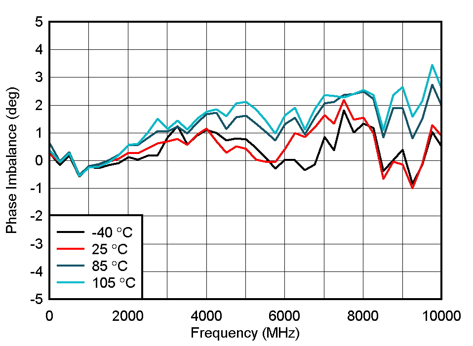
GUID-20210830-SS0I-T7XH-CJZK-P6MWQ1J9BLXH-low.gif
Figure 6-32 Phase Imbalance
GUID-20210830-SS0I-FRTS-ZXRB-NT0T0MTXMFFF-low.svg
Figure 6-34 CMRR Across VDD
GUID-20210922-SS0I-T3LR-6TXZ-GWCRMVQZ2C14-low.svg
Input = +6 dBm
Figure 6-36 Saturation Voltage
GUID-20210923-SS0I-1FJF-NCTZ-J2WV5TG30BKB-low.svg
Figure 6-38 Differential S22