SLWS181K October 2005 – December 2015 TRF3761-A , TRF3761-B , TRF3761-C , TRF3761-E , TRF3761-F , TRF3761-G , TRF3761-H , TRF3761-J
PRODUCTION DATA.
- 1 Features
- 2 Applications
- 3 Description
- 4 Revision History
- 5 Device Comparison Table
- 6 Pin Configuration and Functions
-
7 Specifications
- 7.1 Absolute Maximum Ratings
- 7.2 Recommended Operating Conditions
- 7.3 Thermal Information
- 7.4 Electrical Characteristics
- 7.5 Electrical Characteristics, TRF3761-A
- 7.6 Electrical Characteristics,TRF3761-B
- 7.7 Electrical Characteristics, TRF3761-C
- 7.8 Electrical Characteristics, TRF3761-D
- 7.9 Electrical Characteristics, TRF3761-E
- 7.10 Electrical Characteristics, TRF3761-F
- 7.11 Electrical Characteristics, TRF3761-G
- 7.12 Electrical Characteristics, TRF3761-H
- 7.13 Electrical Characteristics, TRF3761-J
- 7.14 Timing Requirements
- 7.15
Typical Characteristics
- 7.15.1 Typical Characteristics, TRF3761-A (See )
- 7.15.2 Typical Characteristics, TRF3761-B (See )
- 7.15.3 Typical Characteristics, TRF3761-C (See )
- 7.15.4 Typical Characteristics, TRF3761-D (See )
- 7.15.5 Typical Characteristics, TRF3761-E (See )
- 7.15.6 Typical Characteristics, TRF3761-F (See )
- 7.15.7 Typical Characteristics, TRF3761-G (See )
- 7.15.8 Typical Characteristics, TRF3761-H (See )
- 7.15.9 Typical Characteristics, TRF3761-J (See )
-
8 Detailed Description
- 8.1 Overview
- 8.2 Functional Block Diagram
- 8.3 Feature Description
- 8.4 Device Functional Modes
- 8.5 Programming
- 8.6 Register Maps
- 9 Application and Implementation
- 10Power Supply Recommendations
- 11Layout
- 12Device and Documentation Support
- 13Mechanical, Packaging, and Orderable Information
Package Options
Mechanical Data (Package|Pins)
- RHA|40
Thermal pad, mechanical data (Package|Pins)
- RHA|40
Orderable Information
1 Features
- Fully Integrated VCO
- Low Phase Noise: –137dBc/Hz (at 600kHz, fVCO of 1.9GHz)
- Low Noise Floor: –158dBc/Hz at 10MHz Offset
- Integer-N PLL
- Input Reference Frequency range: 10MHz to 104MHz
- VCO Frequency Divided by 2-4 Output
- Output Buffer Enable Pin
- Programmable Charge Pump Current
- Hardware and Software Power Down
- 3-Wire Serial Interface
- Single Supply: 4.5V to 5.25V Operation
2 Applications
- Wireless Infrastructure
- WCDMA, CDMA, GSM
- Wideband Transceivers
- Wireless Local Loop
- RFID Transceivers
- Clock generation
- IF LO generation
3 Description
TRF3761 is a family of high performance, highly integrated frequency synthesizers, optimized for high performance applications. The TRF3761 includes a low-noise, voltage-controlled oscillator (VCO) and an integer-N PLL.
TRF3761 integrates divide-by 1, 2, or 4 options for a more flexible output frequency range. It is controlled through a 3-wire serial-programming-interface (SPI) interface. For power sensitive applications the TRF3761 can be powered down by the SPI interface or externally via chip_en pin 2.
Device Information(1)
| PART NUMBER | PACKAGE | BODY SIZE (NOM) |
|---|---|---|
| TRF3761 | VQFN (40) | 6.00 mm x 6.00 mm |
| TRF3761-x |
- For all available packages, see the orderable addendum at the end of the datasheet.
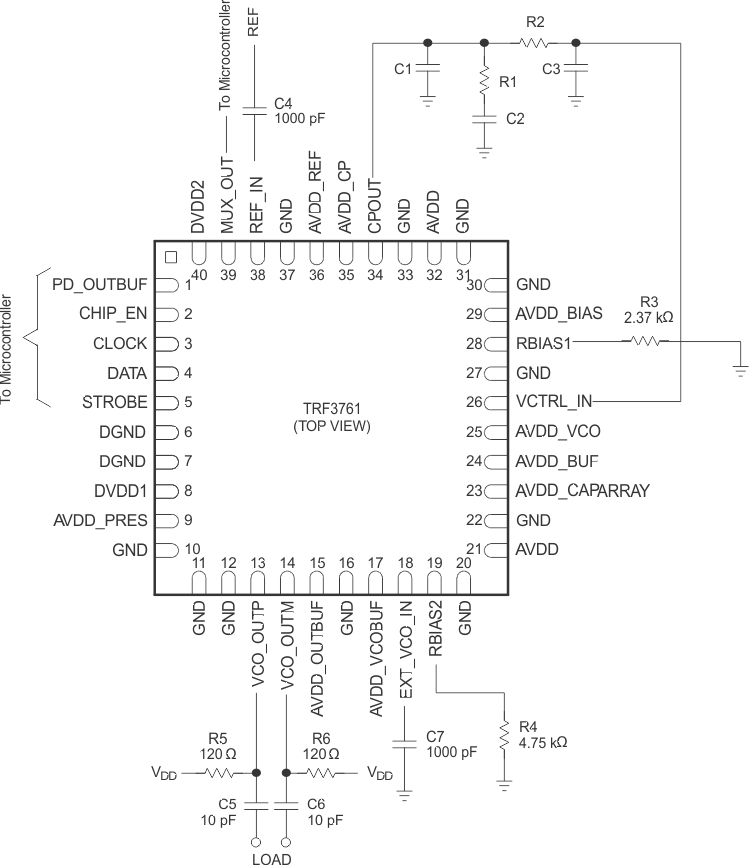
Application Schematic
