SLWS181K October 2005 – December 2015 TRF3761-A , TRF3761-B , TRF3761-C , TRF3761-E , TRF3761-F , TRF3761-G , TRF3761-H , TRF3761-J
PRODUCTION DATA.
- 1 Features
- 2 Applications
- 3 Description
- 4 Revision History
- 5 Device Comparison Table
- 6 Pin Configuration and Functions
-
7 Specifications
- 7.1 Absolute Maximum Ratings
- 7.2 Recommended Operating Conditions
- 7.3 Thermal Information
- 7.4 Electrical Characteristics
- 7.5 Electrical Characteristics, TRF3761-A
- 7.6 Electrical Characteristics,TRF3761-B
- 7.7 Electrical Characteristics, TRF3761-C
- 7.8 Electrical Characteristics, TRF3761-D
- 7.9 Electrical Characteristics, TRF3761-E
- 7.10 Electrical Characteristics, TRF3761-F
- 7.11 Electrical Characteristics, TRF3761-G
- 7.12 Electrical Characteristics, TRF3761-H
- 7.13 Electrical Characteristics, TRF3761-J
- 7.14 Timing Requirements
- 7.15
Typical Characteristics
- 7.15.1 Typical Characteristics, TRF3761-A (See )
- 7.15.2 Typical Characteristics, TRF3761-B (See )
- 7.15.3 Typical Characteristics, TRF3761-C (See )
- 7.15.4 Typical Characteristics, TRF3761-D (See )
- 7.15.5 Typical Characteristics, TRF3761-E (See )
- 7.15.6 Typical Characteristics, TRF3761-F (See )
- 7.15.7 Typical Characteristics, TRF3761-G (See )
- 7.15.8 Typical Characteristics, TRF3761-H (See )
- 7.15.9 Typical Characteristics, TRF3761-J (See )
-
8 Detailed Description
- 8.1 Overview
- 8.2 Functional Block Diagram
- 8.3 Feature Description
- 8.4 Device Functional Modes
- 8.5 Programming
- 8.6 Register Maps
- 9 Application and Implementation
- 10Power Supply Recommendations
- 11Layout
- 12Device and Documentation Support
- 13Mechanical, Packaging, and Orderable Information
Package Options
Mechanical Data (Package|Pins)
- RHA|40
Thermal pad, mechanical data (Package|Pins)
- RHA|40
Orderable Information
9 Application and Implementation
NOTE
Information in the following applications sections is not part of the TI component specification, and TI does not warrant its accuracy or completeness. TI’s customers are responsible for determining suitability of components for their purposes. Customers should validate and test their design implementation to confirm system functionality.
9.1 Application Information
The TRF3761 device is suited for high performance RF transmit signal chain applications such as wireless radio transmitters.
9.1.1 Loop Filter Design
Numerous methodologies and design techniques exist for designing optimized loop filters for particular applications. The loop filter design can affect the stability of the loop, the lock time, the bandwidth, the extra attenuation on the reference spurs, etc. The role of the loop filter is to integrate and lowpass the pulses of the charge pump and eventually yield an output tuning voltage that drives the VCO. Several filter topologies can be implemented, including both passive and active. In this section, a third-order passive filter is used. For this example, assume these several design parameters. The internal VCO has a value of 23MHz/V, meaning that in the linear region, changing the tuning voltage of the VCO by 1V induces a change of the output frequency of about 23MHz. It is known that N = 4500 and Fpfd = 200kHz from our previous example. It is assumed that current setting in register 1 <DB7:DB5> is set to 100 and sets a maximum current of 5.6mA.TI recommends an Icp of 5.6mA, which give the best spur performance, but can be changed for different application. In addition, the bandwidth of the loop filter must be determined. This is a critical consideration as it affects the lock time of the system. Assuming an approximate bandwidth of around 20kHz is required and that for stability a phase margin of about 45 degrees is desired, the following values for the components of the loop filter can be derived. There is almost an infinite number of solutions to the problem of designing the loop filter and the designer is called to make tradeoff decisions for each application. Texas Instruments has provided a loopfilter program in the product folder for the TRF3761.
Some terms are interchangeable and are described and equated here:
- Fcom = FPDF which identify the comparing frequency or phase detector frequency which is also equal to the system channel step size. FOUT must be a multiple of Fcom.
- Fmin is the lower frequency of the design band.
- Fmax is the upper frequency of the design band.
- Fref is the reference frequency for the PLL. Fref must be a multiple of Fcom.
- Kvco = Kv expressed in MHz per Volt (MHz/V) which is the gain of the VCO. The TRF3761 internal VCO has a Kv = 23MHz/V.
- Icp is the charge pump current. The TRF3761 is typically set to 5.6mA.
- Fc is the loop filter bandwidth which should be no more than 1/10 Fcom.
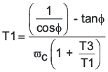
- φ is phase margin in degrees. Values should be between 30 and 70. The higher the phase margin the better the stability of the PLL but the slower the lock time. 45 degrees is a good tradeoff.
- T3/T1 in percent is the percentage of the poles in the loop filter. Usually set to 45%. The higher the value (closer to 100%) the more the spurs are attenuated, but peaking occurs in the pass band of the loop filter.




9.2 Typical Applications
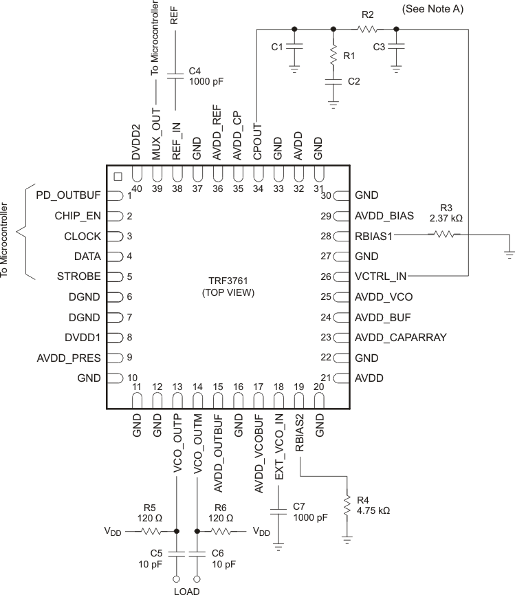
Figure 87 shows a typical application schematic for the TRF3761. In this example, the output signal is taken differential using the 2 resistive pull-up resistors of the final output buffer. A single-ended and tuned load configuration is also available.
The loop filter components:
C1 = 303pF, R1 = 8.87kΩ, C2 = 1650pF, R2 = 3.4kΩ, C3 = 330pF
are the typical values used for the Figure 87. The values can be optimized differently according to the requirements of the different applications.9.2.1 Design Requirements
9.2.1.1 Loop Filter Design Example
Given these parameters which were used for the lock time plot in Figure 88:
- Fmin = 2085 MHz
- Fmax = 2175 MHz
- Fcom = 400 KHz
- Icp = 4.2mA
- Kvco = 23 MHz
- Fc = 20 KHz
- Phase Margin = 45 degrees
- T3/T1 = 45%
Calculate FOUT of design

Next calculate N

Then calculate ωc

Now calculate T1-T3 to give the RC time constants.
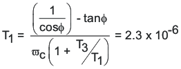
Use T1 to find T3

Then use T1 and T3 to find T2

Now C1, C2, C3, R1, and R2 are calculated using T1, T2, and T3.


Now using C2 and T2, find R2. Use C3 and T3 to find R3


R2 x C3 can be scaled using T3, so if C3 = 330pF, then R2 = 3.03 kΩ => 3.4 kΩ in the loop filter. R1 × C2 can be scaled using T2. Scaling these values helps to improve the lock time. The actual values used in the lock time plot were optimized for lock time as well as using real valued components. The values in figure 62 were taken from the current EVM schematic.
9.2.2 Detailed Design Procedure
9.2.2.1 Initial Calibration and Frequency Setup at Power Up
The integrated high performance VCO requires an internal frequency calibration at power up. To perform such calibration the following procedure is recommended:
- Apply 5V power supply to IC.
- Apply an input reference frequency to pin (38) and ensure the signal is stable.
- Turn on the TRF3761 using the chip enable pin (CHIP_EN, pin 2), by applying 5V.
9.2.2.1.1 Register 1
- Setup the device through Register 1 referencing Table 1.
- The first 4 bits of the 32-bit code sent to the chip are set DB <3:0> to 0000; which is the address of register 1.
- Bit 5, DB4, sets the soft reset for the chip. Soft reset allows for the registers to be reset without powering down the chip. If a soft reset is used then write to register 1 twice: once with DB4 set high and once with DB4 set low. Typically, this bit is only used when the chip has been powered up and registers 1, 2, and 3 have already been written to, so on power-up reset is not required, so DB4 is, by default, set low.
- DB <7: 5> sets the charge pump current based on the resistor value on pin 28 of the TRF3761 and the decimal value of Register 1, DB<7:5> used in Equation 6. This equation reduces to Equation 7, where N = decimal value of [Reg1 DB<7:5>].
- DB <9: 8> sets the mode of the chip. The mode is how the device will or will not divide down the VCO’s frequency. There are 3 choices for the mode setting, divide by 1, 2 or 4 per Table 1. For example, if 393.75MHz is required from the TRF3761 which has a main frequency of 1575MHz then the divide-by-4 mode is chosen by setting DB <9: 8> to 10.
- DB <11:10> controls the output buffer. Both of these are set to 00 by default, so the buffer is controlled internally. Refer to Table 1 for more information.
- DB <25:12> sets the RDiv value. Once the calculations under the Synthesizing a Selected Frequency section have been completed the value is known, based on the external reference oscillator. The value for R is entered into the DB <25:12>. For example, if the reference oscillator is at a frequency (FREF_IN) of 61.44MHz and a channel step size of 120kHz is required, which is also the frequency (FPFD) the phase frequency detector will use to compare against the VCO's output frequency (FOUT), then FREF_IN /FPFD = 512, which is entered as follows: MSB: LSB 0001000000000.
- By default, DB <27:26> are set to 00 for a 1.5ns delay on the anti-backlash pulse width. Refer to Table 1 for more information.
- DB 28 is set to 1 for positive by default. Refer to Table 1 for more information.
- DB 29 is set to 0 for normal operation. Refer to Table 1 for more information.
- DB 30 is set to 0 by default. Refer to Table 1 for more information.
- DB 31 is set to 0 by default. Refer to Table 1 for more information.
9.2.2.1.2 Register 2
- Initiate calibration procedure by programming register 2 as follows: Reference Table 2.
- The first 4 bits of the 32-bit code sent to the chip are set DB <3:0> to 0001; which is the address of register 2.
- Use bits DB<17, 4> of register 2 to specify the input reference frequency in MHz. The value is split into an integer and a fraction part. For example: to insert a fREF of 30.72MHz, set:
- DB<10, 4> (integer part) equal to 0011110 (30) and
- DB<17, 11> (fraction part) equal to 1001000 (72).
- Set DB<30:18> of register 2 to the desired frequency. For example: 2200MHz would be 0100010011000 (2200).
- Set DB31of register 2 to 1 to start the calibration. The VCO calibration runs for 5ms. During the cal procedure it will not be possible to program register 2 and 3. At the end of the calibration, bit DB31 of register 2 resets to 0.
- Subsequent frequency programming requires DB31 to be set to 0.
9.2.2.1.3 Register 3
- Completion of the frequency set up, on initial calibration, cannot proceed until 5ms has elapsed, due to full calibration, then it will require that the A and B values, the prescalar ratio, be known. Refer to Synthesizing a Selected Frequency section for calculation. Reference Table 3.
- The first 4 bits of the 32-bit code sent to the chip are set DB <3:0> to 0010; which is the address of register 3.
- DB<5:4> sets the prescalar ratio, 8/9, 16/17, 32/33, 64/65. For example: if 16/17 are required, set the register bits DB<5:4> to 01.
- DB<11:6> sets the A value for the N counter. For example: if A is 4, set DB<11:6> as follows: 000100 (4).
- DB<24:12> sets the B value for the N counter. For example: if B is 1156, set DB<24:12> as follows: 0010010000100 (4).
- DB<28:25> sets the TEST_MUX. This allows the user to check via the microcontroller the state of the TRF3761 by programming it to one of 6 states. The most common state to use is the Digital lock Detect which places the pin in a logic high state with indicates the VCO is locked.
- DB29 sets the START LOCK, which is set to 0, on the initial frequency setup and then set to 1 on additional frequency changes.
Table 4. MUX-Out Settings
STATE DB<28:25> STATE DB<28:25> 3-state o/p ( High impedance state on Pin 39) 0000 RDiv o/p (Shows R-value on Pin 39) 0100 Digital lock Detect (High when locked on Pin 39) 0001 Analog lock detect (High when locked on Pin 39) 0101 N-Divider o/p (Shows N-value on Pin 39) 0010 Read back ( read back register settings) 0110 DVDD (internal TI use) 0011 DGND (internal TI use) 0111
Once all registers are written, the TRF3761 will lock to the desired frequency. In order to change the frequency once the initial calibration is complete, only registers 2 and 3 need to be reprogrammed. No calibration is required.
9.2.2.2 Re-Calibration After Power Up
Assuming the TRF3761 is powered up and operational, a VCO calibration is also possible without powering down the IC. To perform such calibration the following procedure is recommended:
- Set bit DB4 (RESET) of register 1 to 1. This performs a software reset and clears all registers of VCO calibration data. Once the reset command is issued then DB4 of register 1 will need to be set to 0.
- Repeat the Initial Calibration and Frequency Setup at Power Up section, skipping the power up section and performing the register programming sequence.
9.2.2.3 Synthesizing a Selected Frequency
The TRF3761 is an integer-N PLL synthesizer, and because of its flexibility (14-bit RDiv, 6-bit A counter, 13-bit B counter, and dual modulus prescaler), is ideal for synthesizing virtually any desired frequency. If synthesizing a 900MHz local oscillator, with spacing capability (minimum frequency increment) of 200kHz, as in a typical GSM application, the choice of the external reference oscillator is beyond the scope of this section. However, if a 10MHz reference is selected, the settings are calculated to yield the desired output frequency and channel spacing. There is more than one solution to a specific set of conditions, so below is one way of achieving the desired result. First, select the appropriate RDiv counter value. Since a channel spacing of 200kHz is desired, the FPFD is set to 200kHz. Calculate the RDiv value through:
Assume a prescaler value of 8/9 is selected. This is a valid choice, since the prescaler output is well within the 200MHz limit (900MHz / 8 = 112.5MHz). Select the appropriate A and B counter values.
Therefore, Equation 30 must be solved:
There are many solutions to this single equation with two unknowns; there are some basic constraints on the solution, since 3 ≤ B ≤ 8191, and also B ≥ A. So, if A = 4, solving the equation yields B = 562. One complete solution would be to choose:
RDiv = 50, A counter = 4, Bcounter = 562 and Prescalar = 8/9
resulting in the desired N counter value = 4500. This is how the A counter, B counter and prescalar make up the N counter.
When this procedure is complete the values for the N counter , R, and the prescalar ratio should be known. Registers 2 and 3 need to be set up for operation of the chip. Refer to Table 2 and Table 3 for this procedure. Register 2 bits <DB30:DB18> 12:0 set the output frequency of the device along with register 3. Refer to N-Divider section under the Feature Description.
9.2.3 Application Curve
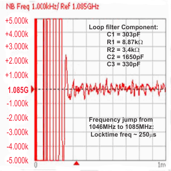 Figure 88. Frequency Locktime
9.2.4 Application Example for a High Performance RF Transmit Signal Chain
Much in the same way as described above, the TRF3761 is an ideal synthesizer to use in implementing a complete high performance RF transmitter chain such as the TSW3000 and TSW3003 Demonstration kits. Using a complete suite of high performance Texas Instruments components, a state-of-the-art transmitter can be implemented featuring excellent performance. Texas Instruments offers ideal solutions for the digital-to-analog conversion portion of transmitter as well as the analog and RF components needed to complete the transmitter. The baseband digital data is converted to I and Q signals through the dual DAC5687, which features a 16-bit interpolating dual digital-to-analog converter (DAC). The device incorporates a digital modulator, independent differential offset control, and I/Q amplitude control. The device is typically used in baseband mode or in low IF mode in conjunction with an analog quadrature modulator. The DAC5687, after filtering, feeds a TRF3703, which is a direct, upconversion IQ modulator. This device accepts a differential input voltage quadrature signal at baseband or low IF frequencies and outputs a modulated RF signal based on the LO drive frequency. The LO drive input of the IQ modulator is generated by the TRF3761. The TRF3761 is a family of high performance, highly integrated frequency synthesizers, optimized for wireless infrastructure applications. The TRF3761 includes an integrated VCO and integer-N PLL. Different members of the TRF3761 family can be chosen for application specific VCO frequency ranges. In addition, the CDC7005 clocking solution can be used to clock the DAC and other portions of the transmitter. A block diagram of the proposed architecture is shown in Figure 89 and Figure 90. For more details, contact Texas Instruments directly.
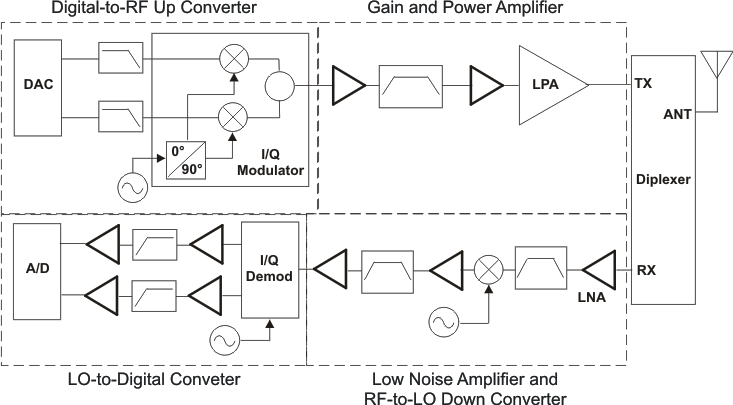 Figure 89. Transmit Chain Block Diagram
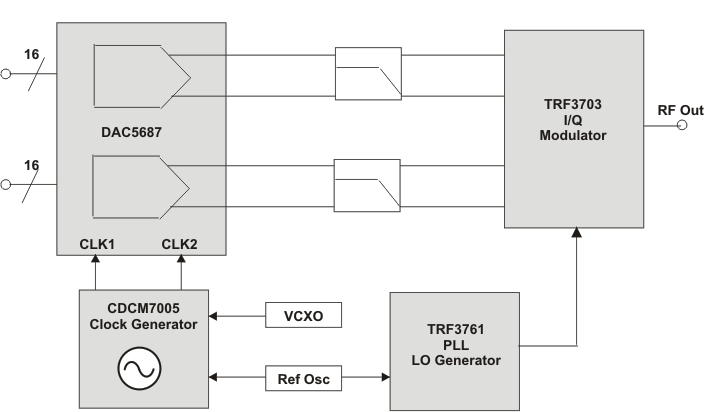 Figure 90. Transmit Chain Block Diagram
