SLOS732G June 2011 – March 2020 TRF7960A
PRODUCTION DATA.
- 1Device Overview
- 2Revision History
- 3Device Characteristics
- 4Terminal Configuration and Functions
- 5Specifications
-
6Detailed Description
- 6.1 Functional Block Diagram
- 6.2 Power Supplies
- 6.3 Supply Arrangements
- 6.4 Supply Regulator Settings
- 6.5 Power Modes
- 6.6 Receiver – Analog Section
- 6.7 Receiver – Digital Section
- 6.8 Oscillator Section
- 6.9 Transmitter - Analog Section
- 6.10 Transmitter - Digital Section
- 6.11 Transmitter – External Power Amplifier or Subcarrier Detector
- 6.12 Communication Interface
- 6.13
Direct Commands from MCU to Reader
- 6.13.1 Command Codes
- 6.13.2 Reset FIFO (0x0F)
- 6.13.3 Transmission With CRC (0x11)
- 6.13.4 Transmission Without CRC (0x10)
- 6.13.5 Delayed Transmission With CRC (0x13)
- 6.13.6 Delayed Transmission Without CRC (0x12)
- 6.13.7 Transmit Next Time Slot (0x14)
- 6.13.8 Block Receiver (0x16)
- 6.13.9 Enable Receiver (0x17)
- 6.13.10 Test Internal RF (RSSI at RX Input With TX On) (0x18)
- 6.13.11 Test External RF (RSSI at RX Input With TX Off) (0x19)
- 6.13.12 Register Preset
- 6.14
Register Description
- 6.14.1
Register Overview
- 6.14.1.1 Main Configuration Registers
- 6.14.1.2
Protocol Subsetting Registers
- 6.14.1.2.1 ISO14443B TX Options Register (0x02)
- 6.14.1.2.2 ISO14443A High-Bit-Rate and Parity Options Register (0x03)
- 6.14.1.2.3 TX Timer High Byte Control Register (0x04)
- 6.14.1.2.4 TX Timer Low Byte Control Register (0x05)
- 6.14.1.2.5 TX Pulse Length Control Register (0x06)
- 6.14.1.2.6 RX No Response Wait Time Register (0x07)
- 6.14.1.2.7 RX Wait Time Register (0x08)
- 6.14.1.2.8 Modulator and SYS_CLK Control Register (0x09)
- 6.14.1.2.9 RX Special Setting Register (0x0A)
- 6.14.1.2.10 Regulator and I/O Control Register (0x0B)
- 6.14.1.3 Status Registers
- 6.14.1.4 Test Registers
- 6.14.1.5 FIFO Control Registers
- 6.14.1
Register Overview
- 7Applications, Implementation, and Layout
- 8Device and Documentation Support
- 9Mechanical, Packaging, and Orderable Information
Package Options
Mechanical Data (Package|Pins)
- RHB|32
Thermal pad, mechanical data (Package|Pins)
- RHB|32
Orderable Information
7.2.2 Impedance Matching TX_Out (Pin 5) to 50 Ω
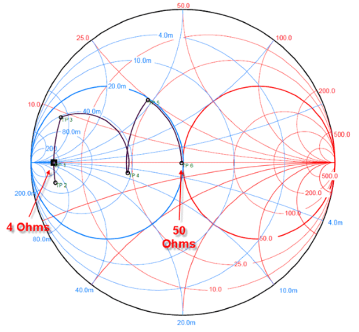
The output impedance of the TRF7960A when operated at full power out setting is nominally 4 + j0 Ω (4 Ω real). This impedance must be matched to a resonant circuit, and TI recommends a matching circuit from 4 Ω to 50 Ω, as commercially available test equipment (for example, spectrum analyzers, power meters, and network analyzers) are 50-Ω systems. See Figure 7-2 and Figure 7-3 for an impedance match reference circuit. This section explains how the values were calculated.
Starting with the 4-Ω source, Figure 7-2 and Figure 7-3 shows the process of going from 4 Ω to 50 Ω by showing it represented on a Smith Chart simulator (available from http://www.fritz.dellsperger.net/). The elements are grouped together where appropriate.
 Figure 7-2 Impedance Matching Circuit
 This yields the following Smith Chart simulation.
 Figure 7-3 Impedance Matching Smith Chart
 Resulting power out can be measured with a power meter, spectrum analyzer with power meter function, or other equipment capable of making a "hot" measurement. Take care to observe maximum power input levels on test equipment and use attenuators whenever available to avoid any possibility of damage to expensive equipment. Table 6-3 lists the expected output power levels under various operating conditions.