SLOS758G December 2011 – March 2020 TRF7963A
PRODUCTION DATA.
- 1Device Overview
- 2Revision History
- 3Device Characteristics
- 4Terminal Configuration and Functions
- 5Specifications
-
6Detailed Description
- 6.1 Functional Block Diagram
- 6.2 Power Supplies
- 6.3 Supply Arrangements
- 6.4 Supply Regulator Settings
- 6.5 Power Modes
- 6.6 Receiver – Analog Section
- 6.7 Receiver – Digital Section
- 6.8 Oscillator Section
- 6.9 Transmitter - Analog Section
- 6.10 Transmitter - Digital Section
- 6.11 Transmitter – External Power Amplifier or Subcarrier Detector
- 6.12 Communication Interface
- 6.13
Direct Commands from MCU to Reader
- 6.13.1 Command Codes
- 6.13.2 Reset FIFO (0x0F)
- 6.13.3 Transmission With CRC (0x11)
- 6.13.4 Transmission Without CRC (0x10)
- 6.13.5 Block Receiver (0x16)
- 6.13.6 Enable Receiver (0x17)
- 6.13.7 Test Internal RF (RSSI at RX Input With TX On) (0x18)
- 6.13.8 Test External RF (RSSI at RX Input With TX Off) (0x19)
- 6.13.9 Register Preset
- 6.14
Register Description
- 6.14.1
Register Overview
- 6.14.1.1 Main Configuration Registers
- 6.14.1.2
Protocol Subsetting Registers
- 6.14.1.2.1 ISO14443B TX Options Register (0x02)
- 6.14.1.2.2 ISO14443A High-Bit-Rate and Parity Options Register (0x03)
- 6.14.1.2.3 TX Pulse Length Control Register (0x06)
- 6.14.1.2.4 RX No Response Wait Time Register (0x07)
- 6.14.1.2.5 RX Wait Time Register (0x08)
- 6.14.1.2.6 Modulator and SYS_CLK Control Register (0x09)
- 6.14.1.2.7 RX Special Setting Register (0x0A)
- 6.14.1.2.8 Regulator and I/O Control Register (0x0B)
- 6.14.1.3 Status Registers
- 6.14.1.4 Test Registers
- 6.14.1.5 FIFO Control Registers
- 6.14.1
Register Overview
- 7Applications, Implementation, and Layout
- 8Device and Documentation Support
- 9Mechanical, Packaging, and Orderable Information
Package Options
Mechanical Data (Package|Pins)
- RHB|32
Thermal pad, mechanical data (Package|Pins)
- RHB|32
Orderable Information
6.7.1.2 External RSSI
The external RSSI is mainly used for test and diagnostic to sense the amplitude of any 13.56-MHz signal at the receiver's RX_IN1 input. The external RSSI measurement is typically done in active mode when the receiver is on but transmitter output is off. The level of the RF signal received at the antenna is measured and stored in the RSSI Levels and Oscillator Status register (0x0F).
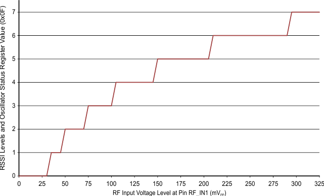
Figure 6-3 shows the relationship between the voltage at the RX_IN1 input and the 3-bit code.
 Figure 6-3 Digital External RSSI Value vs RF Input Level
 The relation between the 3-bit code and the external RF field strength (A/m) sensed by the antenna must be determined by calculation or by experiments for each antenna design. The antenna Q-factor and connection to the RF input influence the result. Direct command 0x19 is used to trigger an internal RSSI measurement.
To check the internal or external RSSI value independent of any other operation:
- Set transmitter to desired state (on or off) using Bit 5 of the Chip Status Control register (0x00) and enable receiver using Bit 1.
- Check internal or external RSSI using direct commands 0x18 or 0x19, respectively. This action places the RSSI value in the RSSI register.
- Delay at least 50 µs.
- Read the RSSI register using direct command 0x0F. Values can range from 0x40 to 0x7F.
- Repeat steps 1 to 4 as desired; the register is reset after read.