SLLS808A JULY 2007 – November 2016 TRS202
UNLESS OTHERWISE NOTED, this document contains PRODUCTION DATA.
- 1 Features
- 2 Applications
- 3 Description
- 4 Revision History
- 5 Pin Configuration and Functions
-
6 Specifications
- 6.1 Absolute Maximum Ratings
- 6.2 ESD Ratings
- 6.3 Recommended Operating Conditions
- 6.4 Thermal Information
- 6.5 Electrical Characteristics
- 6.6 Electrical Characteristics: Driver
- 6.7 Electrical Characteristics: Receiver
- 6.8 Switching Characteristics: Driver
- 6.9 Switching Characteristics: Receiver
- 6.10 Typical Characteristics
- 7 Parameter Measurement Information
- 8 Detailed Description
- 9 Application and Implementation
- 10Power Supply Recommendations
- 11Layout
- 12Device and Documentation Support
- 13Mechanical, Packaging, and Orderable Information
Package Options
Mechanical Data (Package|Pins)
- D|16
Thermal pad, mechanical data (Package|Pins)
Orderable Information
6 Specifications
6.1 Absolute Maximum Ratings
over operating free-air temperature range (unless otherwise noted)(1)| MIN | MAX | UNIT | ||
|---|---|---|---|---|
| Supply voltage, VCC(2) | –0.3 | 6 | V | |
| Positive charge pump voltage, V+(2) | VCC – 0.3 | 14 | V | |
| Negative charge pump voltage, V–(2) | –14 | 0.3 | V | |
| Input voltage, VI | Drivers | –0.3 | V+ + 0.3 | V |
| Receivers | ±30 | |||
| Output voltage, VO | Drivers | V– – 0.3 | V+ + 0.3 | V |
| Receivers | –0.3 | VCC + 0.3 | ||
| Short-circuit duration, DOUT | Continuous | |||
| Operating virtual junction temperature, TJ | 150 | °C | ||
| Storage temperature, Tstg | –65 | 150 | °C | |
(1) Stresses beyond those listed under Absolute Maximum Ratings may cause permanent damage to the device. These are stress ratings only, which do not imply functional operation of the device at these or any other conditions beyond those indicated under Recommended Operating Conditions. Exposure to absolute-maximum-rated conditions for extended periods may affect device reliability.
(2) All voltages are with respect to network GND.
6.2 ESD Ratings
| VALUE | UNIT | ||||
|---|---|---|---|---|---|
| V(ESD) | Electrostatic discharge | Human-body model (HBM), per ANSI/ESDA/JEDEC JS-001(1) | Pins 7, 8, 13, 14, and 15 |
±15000 | V |
| All other pins | ±2000 | ||||
| Charged-device model (CDM), per JEDEC specification JESD22-C101(2) | ±1500 | ||||
(1) JEDEC document JEP155 states that 500-V HBM allows safe manufacturing with a standard ESD control process.
(2) JEDEC document JEP157 states that 250-V CDM allows safe manufacturing with a standard ESD control process.
6.3 Recommended Operating Conditions
see Figure 12(1)| MIN | NOM | MAX | UNIT | |||
|---|---|---|---|---|---|---|
| Supply voltage | 4.5 | 5 | 5.5 | V | ||
| VIH | Driver high-level input voltage (DIN) | 2 | V | |||
| VIL | Driver low-level input voltage (DIN) | 0.8 | V | |||
| VI | Driver input voltage (DIN) | 0 | 5.5 | V | ||
| Receiver input voltage (RIN) | –30 | 30 | ||||
| TA | Operating free-air temperature | TRS202C | 0 | 70 | °C | |
| TRS202I | –40 | 85 | ||||
(1) Test conditions are C1 to C4 = 0.1 µF at VCC = 5 V ±0.5 V.
6.4 Thermal Information
| THERMAL METRIC(1) | TRS202 | UNIT | ||
|---|---|---|---|---|
| D (SOIC) | PW (TSSOP) | |||
| 16 PINS | 16 PINS | |||
| RθJA | Junction-to-ambient thermal resistance | 76.2 | 101 | °C/W |
| RθJC(top) | Junction-to-case (top) thermal resistance | 36.8 | 36.4 | °C/W |
| RθJB | Junction-to-board thermal resistance | 33.9 | 45.9 | °C/W |
| ψJT | Junction-to-top characterization parameter | 6.7 | 2.7 | °C/W |
| ψJB | Junction-to-board characterization parameter | 33.6 | 45.3 | °C/W |
(1) For more information about traditional and new thermal metrics, see the Semiconductor and IC Package Thermal Metrics application report.
6.5 Electrical Characteristics
over recommended ranges of supply voltage and operating free-air temperature (unless otherwise noted; see Figure 12)(1)| PARAMETER | TEST CONDITIONS | MIN | TYP(2) | MAX | UNIT | |
|---|---|---|---|---|---|---|
| ICC | Supply current | No load and VCC = 5 V | 8 | 15 | mA | |
(1) Test conditions are C1 to C4 = 0.1 µF at VCC = 5 V ±0.5 V.
(2) All typical values are at VCC = 5 V and TA = 25°C.
6.6 Electrical Characteristics: Driver
over recommended ranges of supply voltage and operating free-air temperature (unless otherwise noted; see Figure 12)(1)| PARAMETER | TEST CONDITIONS | MIN | TYP(2) | MAX | UNIT | ||
|---|---|---|---|---|---|---|---|
| VOH | High-level output voltage | DOUT at RL = 3 kΩ to GND and DIN = GND | 5 | 9 | V | ||
| VOL | Low-level output voltage | DOUT at RL = 3 kΩ to GND and DIN = VCC | –5 | –9 | V | ||
| IIH | High-level input current | VI = VCC | 15 | 200 | µA | ||
| IIL | Low-level input current | VI at 0 V | –15 | –200 | µA | ||
| IOS(3) | Short-circuit output current | VCC = 5.5 V and VO = 0 V | ±10 | ±60 | mA | ||
| ro | Output resistance | VCC, V+, V– = 0 V, and VO = ±2 V | 300 | Ω | |||
(1) Test conditions are C1 to C4 = 0.1 µF at VCC = 5 V ±0.5 V.
(2) All typical values are at VCC = 5 V and TA = 25°C.
(3) Short-circuit durations must be controlled to prevent exceeding the device absolute power dissipation ratings, and not more than one output must be shorted at a time.
6.7 Electrical Characteristics: Receiver
over recommended ranges of supply voltage and operating free-air temperature (unless otherwise noted; see Figure 12)(1)| PARAMETER | TEST CONDITIONS | MIN | TYP(2) | MAX | UNIT | ||
|---|---|---|---|---|---|---|---|
| VOH | High-level output voltage | IOH = –1 mA | 3.5 | VCC – 0.4 | V | ||
| VOL | Low-level output voltage | IOL = 1.6 mA | 0.4 | V | |||
| VIT+ | Positive-going input threshold voltage | VCC = 5 V and TA = 25°C | 1.7 | 2.4 | V | ||
| VIT– | Negative-going input threshold voltage | VCC = 5 V and TA = 25°C | 0.8 | 1.2 | V | ||
| Vhys | Input hysteresis (VIT+ – VIT–) | 0.2 | 0.5 | 1 | V | ||
| rI | Input resistance | VI = ±3 V to ±25 V | 3 | 5 | 7 | kΩ | |
(1) Test conditions are C1 to C4 = 0.1 µF at VCC = 5 V ±0.5 V.
(2) All typical values are at VCC = 5 V and TA = 25°C.
6.8 Switching Characteristics: Driver
over recommended ranges of supply voltage and operating free-air temperature (unless otherwise noted; see Figure 12)(1)| PARAMETER | TEST CONDITIONS | MIN | TYP(2) | MAX | UNIT | ||
|---|---|---|---|---|---|---|---|
| Maximum data rate | CL = 50 to 1000 pF, one DOUT switching, and RL = 3 kΩ to 7 kΩ (see Figure 6) |
120 | kbit/s | ||||
| tPLH(D) | Propagation delay time, low- to high-level output |
CL = 2500 pF, all drivers loaded, and RL = 3 kΩ (see Figure 6) |
2 | µs | |||
| tPHL(D) | Propagation delay time, high- to low-level output |
CL = 2500 pF, all drivers loaded, and RL = 3 kΩ (see Figure 6) |
2 | µs | |||
| tsk(p) | Pulse skew(3) | CL = 150 pF to 2500 pF and RL = 3 kΩ to 7 kΩ (see Figure 7) |
300 | ns | |||
| SR(tr) | Slew rate, transition region | CL = 50 pF to 1000 pF, VCC = 5 V, and RL = 3 kΩ to 7 kΩ (see Figure 6) | 3 | 6 | 30 | V/µs | |
(1) Test conditions are C1 to C4 = 0.1 µF at VCC = 5 V ±0.5 V.
(2) All typical values are at VCC = 5 V and TA = 25°C.
(3) Pulse skew is defined as |tPLH – tPHL| of each channel of the same device.
6.9 Switching Characteristics: Receiver
over recommended ranges of supply voltage and operating free-air temperature (unless otherwise noted; see Figure 8)(1)| PARAMETER | TEST CONDITIONS | MIN | TYP(2) | MAX | UNIT | |
|---|---|---|---|---|---|---|
| tPLH(R) | Propagation delay time, low- to high-level output | CL = 150 pF | 0.5 | 10 | µs | |
| tPHL(R) | Propagation delay time, high- to low-level output | CL = 150 pF | 0.5 | 10 | µs | |
| tsk(p) | Pulse skew(3) | 300 | ns | |||
(1) Test conditions are C1 to C4 = 0.1 µF at VCC = 5 V ±0.5 V.
(2) All typical values are at VCC = 5 V and TA = 25°C.
(3) Pulse skew is defined as |tPLH – tPHL| of each channel of the same device.
6.10 Typical Characteristics
TA = 25°C (unless otherwise noted)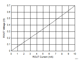 Figure 1. Receiver VOL vs Output Current
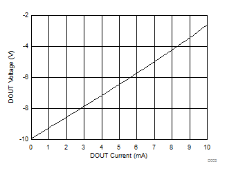 Figure 3. Driver VOL vs Output Current
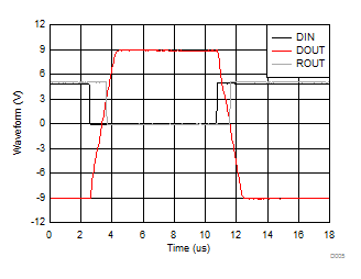 Figure 5. Driver and Receiver Loopback Waveforms
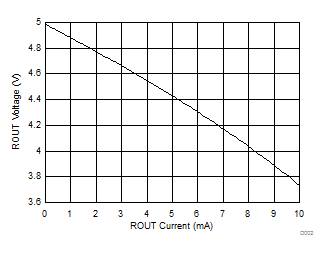 Figure 2. Receiver VOH vs Output Current
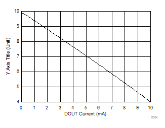 Figure 4. Driver VOH vs Output Current