SLLS807A June 2007 – July 2024 TRS213
PRODUCTION DATA
- 1
- 1 Features
- 2 Applications
- 3 Description
- 4 Pin Configuration and Functions
-
5 Specifications
- 5.1 Absolute Maximum Ratings
- 5.2 Recommended Operating Conditions
- 5.3 Thermal Information
- 5.4 Electrical Characteristics
- 5.5 Electrical Characteristics, Driver
- 5.6 Switching Characteristics, Driver
- 5.7 ESD Protection, Driver
- 5.8 Electrical Characteristics, Receiver
- 5.9 Switching Characteristics, Receiver
- 5.10 ESD Protection, Receiver
- 6 Parameter Measurement Information
- 7 Functional Modes
- 8 Application and Implementation
- 9 Device and Documentation Support
- 10Revision History
- 11Mechanical, Packaging, and Orderable Information
Package Options
Refer to the PDF data sheet for device specific package drawings
Mechanical Data (Package|Pins)
- DB|28
- DW|28
Thermal pad, mechanical data (Package|Pins)
Orderable Information
3 Description
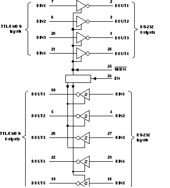
The TRS213 device consists of four line drivers, five line receivers, and a dual charge-pump circuit with ±15kV ESD protection pin to pin (serial-port connection pins, including GND). The device meets the requirements of TIA/EIA-232-F and provides the electrical interface between an asynchronous communication controller and the serial-port connector. The charge pump and four small external capacitors allow operation from a single 5V supply. The devices operate at data signaling rates up to 120kbit/s and a maximum of 30V/μs driver output slew rate.
The TRS213 has an active-low shutdown ( SHDN) and an active-high enable control (EN). In shutdown mode, the charge pumps are turned off, V+ is pulled down to VCC, V– is pulled to GND, and the transmitter outputs are disabled. This reduces supply current typically to 1μA. Two receivers of the TRS213 are active during shutdown.
| PART NUMBER | PACKAGE(1) | PACKAGE SIZE(2) |
|---|---|---|
| TRS213 | DB (SSOP) | 10.2 mm x 7.8mm |
| DW (SOIC) | 17.9mm x 10.3mm |
 Logic Diagram (Positive Logic)