SLLS790E June 2007 – December 2024 TRS3232E
PRODUCTION DATA
- 1
- 1 Features
- 2 Applications
- 3 Description
- 4 Pin Configuration and Functions
-
5 Specifications
- 5.1 Absolute Maximum Ratings
- 5.2 ESD Ratings
- 5.3 ESD Ratings - IEC Specifications
- 5.4 Recommended Operating Conditions
- 5.5 Thermal Information
- 5.6 Electrical Characteristics — Device
- 5.7 Electrical Characteristics — Driver
- 5.8 Electrical Characteristics — Receiver
- 5.9 Switching Characteristics
- Typical Characteristics
- 6 Parameter Measurement Information
- 7 Detailed Description
- 8 Application and Implementation
- 9 Device and Documentation Support
- 10Revision History
- 11Mechanical, Packaging, and Orderable Information
Package Options
Mechanical Data (Package|Pins)
Thermal pad, mechanical data (Package|Pins)
Orderable Information
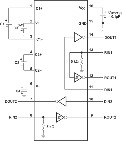
8.2 Typical Application
ROUT and DIN connect to UART or general-purpose logic lines. RIN and DOUT lines connect to a RS232 connector or cable. For proper operation, add capacitors as shown in Table 8-1.

A. C3 can be connected to
VCC or GND
Resistor values
shown are nominal.
Nonpolorized
ceramic capacitors are acceptable. If polarized tantalum or electrolytic
capacitors are used, they should be connected as shown.
Figure 8-1 Typical
Operating Circuit and Capacitor ValuesTable 8-1 VCC vs Capacitor Values
| VCC | C1 | C2, C3, C4 | ||
|---|---|---|---|---|
| 3.3V ± 0.3V | 0.1µF | 0.1µF | ||
| 5V ± 0.5V | 0.047µF | 0.33µF | ||
| 3V ± 5.5V | 0.1µF | 0.47µF | ||