SLLS790E June 2007 – December 2024 TRS3232E
PRODUCTION DATA
- 1
- 1 Features
- 2 Applications
- 3 Description
- 4 Pin Configuration and Functions
-
5 Specifications
- 5.1 Absolute Maximum Ratings
- 5.2 ESD Ratings
- 5.3 ESD Ratings - IEC Specifications
- 5.4 Recommended Operating Conditions
- 5.5 Thermal Information
- 5.6 Electrical Characteristics — Device
- 5.7 Electrical Characteristics — Driver
- 5.8 Electrical Characteristics — Receiver
- 5.9 Switching Characteristics
- Typical Characteristics
- 6 Parameter Measurement Information
- 7 Detailed Description
- 8 Application and Implementation
- 9 Device and Documentation Support
- 10Revision History
- 11Mechanical, Packaging, and Orderable Information
Package Options
Mechanical Data (Package|Pins)
Thermal pad, mechanical data (Package|Pins)
Orderable Information
Abstract
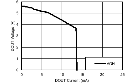
| VCC = 3.3V |
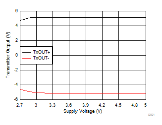
| TX1 at 250kbps | TX2 at 15.6kbps | ||
| Both TX loaded 3kΩ and 100pF | |||
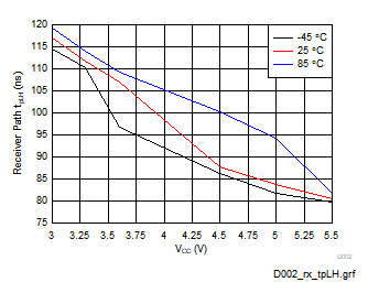 Figure 5-5 Receiver Path Low-to-High Propagation Delay
 (RGT Package)
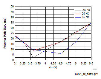 Figure 5-7 Receiver Path Skew (|tpHL-tpLH|) (RGT
Package)
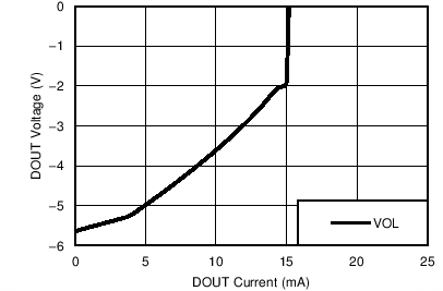
| VCC = 3.3V |
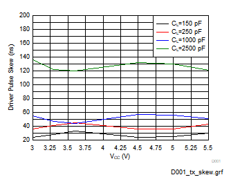 Figure 5-4 Driver Pulse Skew (RGT Package)
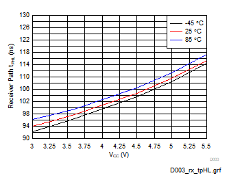 Figure 5-6 Receiver Path High-to-Low Propagation Delay
(RGT Package)