SLLS790D June 2007 – June 2021 TRS3232E
PRODUCTION DATA
- 1 Features
- 2 Applications
- 3 Description
- 4 Revision History
- 5 Pin Configuration and Functions
- 6 Specifications
- 7 Parameter Measurement Information
- 8 Detailed Description
- 9 Application and Implementation
- 10Power Supply Recommendations
- 11Layout
- 12Device and Documentation Support
- 13Mechanical, Packaging, and Orderable Information
Package Options
Mechanical Data (Package|Pins)
Thermal pad, mechanical data (Package|Pins)
Orderable Information
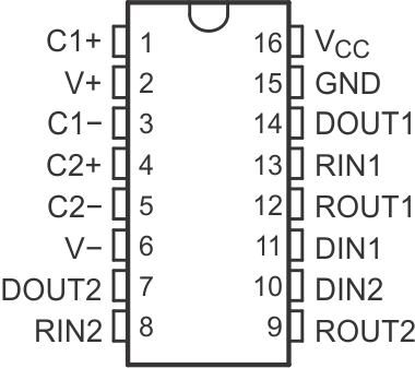
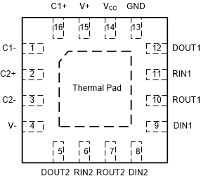
5 Pin Configuration and Functions
 Figure 5-1 D, DW, DB or PW Package,
16-Pin SOIC, SSOP or TSSOP, Top View
 Figure 5-2 RGT package, 16 Pin VQFN, Top View
Table 5-1 Pin Functions
| PIN | I/O | DESCRIPTION | ||
|---|---|---|---|---|
| NAME | NO. |
RGT |
||
| C1+ | 1 |
16 |
— | Positive lead of C1 capacitor |
| C1– | 3 |
1 |
— | Negative lead of C1 capacitor |
| C2+ | 4 |
2 |
— | Positive lead of C2 capacitor |
| C2– | 5 |
3 |
— | Negative lead of C2 capacitor |
| DIN1 | 11 |
9 |
I | Logic data input (from UART) |
| DIN2 | 10 |
8 |
I | Logic data input (from UART) |
| DOUT2 | 7 |
5 |
O | RS232 line data output (to remote RS232 system) |
| DOUT1 | 14 |
12 |
O | RS232 line data output (to remote RS232 system) |
| GND | 15 |
13 |
— | Ground |
| RIN1 | 13 |
11 |
I | RS232 line data input (from remote RS232 system) |
| RIN2 | 8 |
6 |
I | RS232 line data input (from remote RS232 system) |
| ROUT2 | 9 |
7 |
O | Logic data output (to UART) |
| ROUT1 | 12 |
10 |
O | Logic data output (to UART) |
| V+ | 2 |
15 |
O | Positive charge pump output for storage capacitor only |
| V– | 6 |
4 |
O | Negative charge pump output for storage capacitor only |
| VCC | 16 |
14 |
— | Supply voltage, connect to external 3-V to 5.5-V power supply |
| Thermal Pad | Yes | — | Thermal pad for improving heat dissipation. Can be connected to GND or left floating. | |