-
TRS3253E RS-232 Transceiver With Split Supply Pin for Logic Side
- 1 Features
- 2 Applications
- 3 Description
- 4 Revision History
- 5 Pin Configuration and Functions
-
6 Specifications
- 6.1 Absolute Maximum Ratings
- 6.2 ESD Ratings
- 6.3 Recommended Operating Conditions
- 6.4 Thermal Information
- 6.5 Electrical Characteristics—Power
- 6.6 Electrical Characteristics—Driver
- 6.7 Electrical Characteristics—Receiver
- 6.8 Electrical Characteristics—Status
- 6.9 Switching Characteristics—Driver
- 6.10 Switching Characteristics—Receiver
- 6.11 Switching Characteristics—Power and Status
- 6.12 Typical Characteristics
- 7 Parameter Measurement Information
- 8 Detailed Description
- 9 Application and Implementation
- 10Power Supply Recommendations
- 11Layout
- 12Device and Documentation Support
- 13Mechanical, Packaging, and Orderable Information
- IMPORTANT NOTICE
Package Options
Mechanical Data (Package|Pins)
- RSM|32
Thermal pad, mechanical data (Package|Pins)
- RSM|32
Orderable Information
TRS3253E RS-232 Transceiver With Split Supply Pin for Logic Side
1 Features
- VL Pin for Compatibility With Mixed-Voltage Systems Down to 1.8 V on Logic Side
- Enhanced ESD Protection on RIN Inputs and DOUT Outputs
- ±15-kV IEC 61000-4-2 Air-Gap Discharge
- ±8-kV IEC 61000-4-2 Contact Discharge
- ±15-kV Human Body Model
- Low 300-μA Supply Current
- Specified 1000-kbps Data Rate
- Auto Powerdown Plus Feature
2 Applications
- Hand-Held Equipment
- Cell Phones
- Battery-Powered Equipment
- Data Cables
- POS Equipment
- HDMI Switch Matrix
- Debug Ports
3 Description
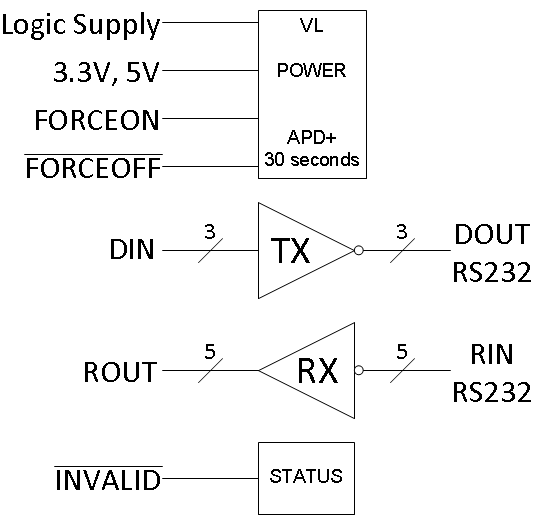
The TRS3253E device is a three-driver and five-receiver RS-232 interface device, with split supply pins for mixed-signal operations without needing an external voltage translator. All RS-232 inputs and outputs are protected to ±15 kV using the IEC 61000-4-2 Air-Gap Discharge method, ±8 kV using the IEC 61000-4-2 Contact Discharge method, and ±15 kV using the Human Body Model.
The charge pump requires only four capacitors for operation from a single 3.3-V or 5-V supply. The TRS3253E is capable of running at data rates up to 1000 kbps, while maintaining RS-232 compliant output levels.
The TRS3253E is available in a space-saving VQFN package (4-mm × 4-mm RSM).
Auto-powerdown-plus automatically powers down drivers to reduce power after 30 seconds of inactivity. In powerdown state supply current is 10 μA maximum.
Receiver input voltage status is available on INVALID logic output even when the device is in powerdown state.
Device Information(1)
| PART NUMBER | PACKAGE | BODY SIZE (NOM) |
|---|---|---|
| TRS3253ERSM | VQFN (32) | 2.80 mm × 2.80 mm |
- For all available packages, see the orderable addendum at the end of the data sheet.
Simplified Diagram
4 Revision History
Changes from C Revision (June 2015) to D Revision
- Changed "IEC61000-4-2, Contact Discharge" from "8 kV" to "15 kV" in Features, Description, Overview and ESD RatingsGo
Changes from B Revision (December 2013) to C Revision
- Added Device Information table, Pin Functions table, ESD Ratings table, Thermal Information table, Typical Characteristics, Feature Description section, Device Functional Modes, Application and Implementation section, Power Supply Recommendations section, Layout section, Device and Documentation Support section, and Mechanical, Packaging, and Orderable Information section.Go
5 Pin Configuration and Functions

Pin Functions
| PIN | I/O | DESCRIPTION | |
|---|---|---|---|
| NAME | NO. | ||
| C1+ | 29 | — | Positive terminals of the voltage-doubler charge-pump capacitors |
| C2+ | 1 | ||
| C1– | 31 | — | Negative terminals of the voltage-doubler charge-pump capacitors |
| C2– | 2 | ||
| DIN1 | 4 | I | Driver inputs |
| DIN2 | 5 | ||
| DIN3 | 7 | ||
| DOUT1 | 25 | O | RS-232 driver outputs |
| DOUT2 | 23 | ||
| DOUT3 | 22 | ||
| FORCEOFF | 28 | I | Auto-powerdown-plus control input |
| FORCEON | 9 | I | Auto-powerdown-plus control input |
| GND | 26 | — | Ground |
| INVALID | 6 | O | Invalid output pin. Active low when all RIN inputs are unpowered |
| NC | 8 | — | No connect pins (do not connect to these pins) |
| 16 | |||
| 24 | |||
| 32 | |||
| RIN1 | 21 | I | RS-232 receiver inputs |
| RIN2 | 20 | ||
| RIN3 | 19 | ||
| RIN4 | 18 | ||
| RIN5 | 17 | ||
| ROUT1 | 14 | O | Receiver outputs. Swing between 0 and VL |
| ROUT2 | 13 | ||
| ROUT3 | 12 | ||
| ROUT4 | 11 | ||
| ROUT5 | 10 | ||
| VCC | 27 | — | 3-V to 5.5-V supply voltage |
| VL | 15 | — | Logic-level supply. All CMOS inputs and outputs are referenced to this supply |
| V+ | 30 | O | 5.5-V supply generated by the charge pump |
| V– | 3 | O | –5.5-V supply generated by the charge pump |
6 Specifications
6.1 Absolute Maximum Ratings
over operating free-air temperature range (unless otherwise noted)(1)| MIN | MAX | UNIT | |||
|---|---|---|---|---|---|
| VCC to GND | –0.3 | 6 | V | ||
| VL to GND | –0.3 | VCC + 0.3 | |||
| V+ to GND | –0.3 | 7 | |||
| V– to GND | 0.3 | –7 | |||
| V+ + |V–|(2) | 13 | ||||
| VI | Input voltage | DIN, FORCEOFF, and FORCEON to GND | –0.3 | 6 | V |
| RIN to GND | ±25 | ||||
| VO | Output voltage | DOUT to GND | ±13.2 | V | |
| ROUT to GND | –0.3 | VL + 0.3 | |||
| Continuous power dissipation | TA = 85°C, 32-pin RSM (RθJA = 37.2°C/W)(3) | 1747 | mW | ||
| TJ | Junction temperature | 150 | °C | ||
| Tstg | Storage temperature | –65 | 150 | °C | |
6.2 ESD Ratings
| VALUE | UNIT | ||||
|---|---|---|---|---|---|
| V(ESD) | Electrostatic discharge | Human body model (HBM), per ANSI/ESDA/JEDEC JS-001(1) | All pins except 17 to 23 and 25 | ±2000 | V |
| Pins 17 to 23 and 25 | ±15000 | ||||
| Charged-device model (CDM), per JEDEC specification JESD22-C101(2) | All pins | ±1500 | |||
| IEC61000-4-2, Contact discharge | Pins 17 to 23 and 25 | ±8000 | |||
| IEC61000-4-2, Air-gap discharge | Pins 17 to 23 and 25 | ±15000 | |||
6.3 Recommended Operating Conditions
| MIN | MAX | UNIT | ||||
|---|---|---|---|---|---|---|
| VCC | Supply voltage | 3 | 5.5 | V | ||
| VL | Supply voltage | 1.65 | VCC | V | ||
| Input logic low | DIN, FORCEOFF, FORCEON | VL = 3 V or 5.5 V | 0 | 0.8 | V | |
| VL = 2.3 V | 0 | 0.6 | ||||
| VL = 1.65 V | 0 | 0.5 | ||||
| Input logic high | DIN, FORCEOFF, FORCEON | VL = 5.5 V | 2.4 | VL | V | |
| VL = 3 V | 2 | VL | ||||
| VL = 2.7 V | 1.4 | VL | ||||
| VL = 1.95 V | 1.25 | VL | ||||
| Operating temperature | TRS3253EIRSMR | –40 | 85 | °C | ||
| Receiver input voltage | –25 | 25 | V | |||
6.4 Thermal Information
| THERMAL METRIC(1) | TRS3253E | UNIT | |
|---|---|---|---|
| RSM (VQFN) | |||
| 32 PINS | |||
| RθJA | Junction-to-ambient thermal resistance | 37.2 | °C/W |
| RθJC(top) | Junction-to-case (top) thermal resistance | 30.1 | °C/W |
| RθJB | Junction-to-board thermal resistance | 7.8 | °C/W |
| ψJT | Junction-to-top characterization parameter | 0.4 | °C/W |
| ψJB | Junction-to-board characterization parameter | 7.6 | °C/W |
| RθJC(bot) | Junction-to-case (bottom) thermal resistance | 2.4 | °C/W |
6.5 Electrical Characteristics—Power
over operating free-air temperature range, VCC = VL = 3 V to 5.5 V, C1–C4 = 0.1 μF (tested at 3.3 V ± 10%), C1 = 0.047 μF, C2–C4 = 0.33 μF (tested at 5 V ± 10%) (unless otherwise noted)(1)| PARAMETER | TEST CONDITIONS | MIN | TYP(2) | MAX | UNIT | ||
|---|---|---|---|---|---|---|---|
| II | Input leakage current | FORCEOFF, FORCEON | ±0.01 | ±1 | μA | ||
| ICC | Supply current (TA = 25°C) |
Auto-powerdown plus disabled | No load, FORCEOFF and FORCEON at VCC |
0.5 | 1 | mA | |
| Powered off | No load, FORCEOFF at GND | 1 | 10 | μA | |||
| Auto-powerdown plus active | No load, FORCEOFF at VCC, FORCEON at GND, All RIN are open or grounded |
1 | 10 | ||||
6.6 Electrical Characteristics—Driver
over operating free-air temperature range, VCC = VL = 3 V to 5.5 V, C1–C4 = 0.1 μF (tested at 3.3 V ± 10%), C1 = 0.047 μF, C2–C4 = 0.33 μF (tested at 5 V ± 10%), TA = TMIN to TMAX (unless otherwise noted)| PARAMETER | TEST CONDITIONS | MIN | TYP(1) | MAX | UNIT | |
|---|---|---|---|---|---|---|
| VOH | Output voltage swing | All driver outputs loaded with 3 kΩ to ground, VCC= 3.1V to 5.5V | ±5 | ±5.4 | V | |
| rO | Output resistance | VCC = V+ = V– = 0, Driver output = ±2 V | 300 | 10M | Ω | |
| IOS | Output short-circuit current | VT_OUT = 0 | ±60 | mA | ||
| IOZ | Output leakage current | VT_OUT = ±12 V, FORCEOFF = GND, VCC = 3 V to 3.6 V |
±25 | μA | ||
| VT_OUT = ±12 V, FORCEOFF = GND, VCC = 4.5 V to 5.5 V |
||||||
| Driver input hysteresis | 0.5 | V | ||||
| Input leakage current | DIN, FORCEOFF, FORCEON | ±0.01 | ±1 | μA | ||
6.7 Electrical Characteristics—Receiver
over operating free-air temperature range, VCC = VL = 3 V to 5.5 V, C1–C4 = 0.1 μF (tested at 3.3 V ± 10%), C1 = 0.047 μF, C2–C4 = 0.33 μF (tested at 5 V ± 10%), TA = TMIN to TMAX (unless otherwise noted)| PARAMETER | TEST CONDITIONS | MIN | TYP(1) | MAX | UNIT | ||
|---|---|---|---|---|---|---|---|
| Ioff | Output leakage current | ROUT, receivers disabled | ±0.05 | ±10 | μA | ||
| VOL | Output voltage low | IOUT = 1.6 mA | 0.4 | V | |||
| VOH | Output voltage high | IOUT = –1 mA | VL – 0.6 | VL – 0.1 | V | ||
| VIT– | Input threshold low | TA = 25°C | VL = 5 V | 0.8 | 1.2 | V | |
| VL = 3.3 V | 0.6 | 1.5 | |||||
| VIT+ | Input threshold high | TA = 25°C | VL = 5 V | 1.8 | 2.4 | V | |
| VL = 3.3 V | 1.5 | 2.4 | |||||
| Vhys | Input hysteresis | 0.5 | V | ||||
| Input resistance | TA = 25°C | 3 | 5 | 7 | kΩ | ||
6.8 Electrical Characteristics—Status
over recommended ranges of supply voltage and operating free-air temperature (unless otherwise noted)| PARAMETER | TEST CONDITIONS | MIN | MAX | UNIT | |
|---|---|---|---|---|---|
| VIT+(valid) | Receiver input threshold for INVALID high-level output voltage |
FORCEON = GND, FORCEOFF = VL | 2.7 | V | |
| VIT–(valid) | Receiver input threshold for INVALID high-level output voltage |
FORCEON = GND, FORCEOFF = VL | –2.7 | V | |
| VT(invalid) | Receiver input threshold for INVALID low-level output voltage |
FORCEON = GND, FORCEOFF = VL | –0.3 | 0.3 | V |
| VOH | INVALID high-level output voltage | IOH = –1 mA, FORCEON = GND, FORCEOFF = VL |
VL – 0.6 | V | |
| VOL | INVALID low-level output voltage | IOL = 1.6 mA, FORCEON = GND, FORCEOFF = VL |
0.4 | V | |
6.9 Switching Characteristics—Driver
over operating free-air temperature range, VCC = VL = 3 V to 5.5 V, C1–C4 = 0.1 μF (tested at 3.3 V ± 10%), C1 = 0.047 μF, C2–C4 = 0.33 μF (tested at 5 V ± 10%), TA = TMIN to TMAX (unless otherwise noted)| PARAMETER | TEST CONDITIONS | MIN | TYP(1) | MAX | UNIT | ||
|---|---|---|---|---|---|---|---|
| Maximum data rate | RL = 3 kΩ, CL = 200 pF, one driver switching | 1000 | kbps | ||||
| Time-to-exit powerdown | |VT_OUT| > 3.7 V | 100 | μs | ||||
| |tPHL – tPLH| | Driver skew(2) | 100 | ns | ||||
| Transition-region slew rate |
VCC = 3.3 V, TA = 25°C, RL = 3 kΩ to 7 kΩ, Measured from 3 V to –3 V or –3 V to 3 V |
CL = 150 pF to 1000 pF | 15 | 150 | V/μs | ||
6.10 Switching Characteristics—Receiver
over operating free-air temperature range, VCC = VL = 3 V to 5.5 V, C1–C4 = 0.1 μF (tested at 3.3 V ± 10%), C1 = 0.047 μF, C2–C4 = 0.33 μF (tested at 5 V ± 10%), TA = TMIN to TMAX (unless otherwise noted)| PARAMETER | TEST CONDITIONS | MIN | TYP(1) | MAX | UNIT | |
|---|---|---|---|---|---|---|
| tPHL | Receiver propagation delay | Receiver input to receiver output, CL = 150 pF | 0.15 | μs | ||
| tPLH | 0.15 | |||||
| tPHL – tPLH | Receiver skew | 50 | ns | |||
| ten | Receiver output enable time | From FORCEOFF | 200 | |||
| tdis | Receiver output disable time | From FORCEOFF | 200 | |||
6.11 Switching Characteristics—Power and Status
over recommended ranges of supply voltage and operating free-air temperature (unless otherwise noted) (see Figure 7)| PARAMETER | MIN | TYP(1) | MAX | UNIT | |
|---|---|---|---|---|---|
| tvalid | Propagation delay time, low- to high-level output | 0.1 | μs | ||
| tinvalid | Propagation delay time, high- to low-level output | 50 | |||
| ten | Supply enable time | 25 | |||
| tdis | Receiver or driver edge to auto-powerdown plus | 15 | 30 | 60 | s |
6.12 Typical Characteristics
VCC = 3.3 V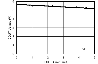
Other Drivers 3-kΩ Load
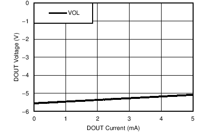
Other Drivers 3-kΩ Load
7 Parameter Measurement Information

tf ≤ 10 ns.

tf ≤ 10 ns.

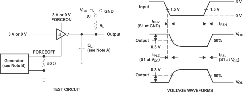
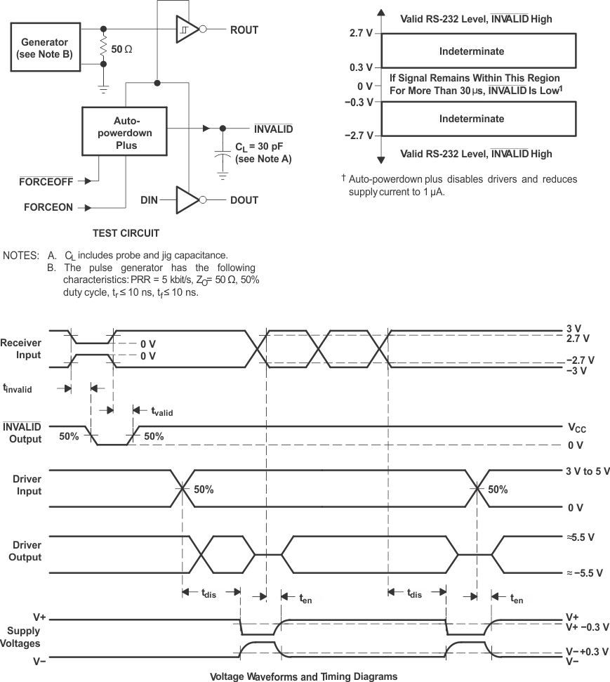 Figure 7. INVALID Propagation-Delay Times and Supply-Enabling Time