SLLS850D January 2008 – March 2017 TRS3253E
PRODUCTION DATA.
- 1 Features
- 2 Applications
- 3 Description
- 4 Revision History
- 5 Pin Configuration and Functions
-
6 Specifications
- 6.1 Absolute Maximum Ratings
- 6.2 ESD Ratings
- 6.3 Recommended Operating Conditions
- 6.4 Thermal Information
- 6.5 Electrical Characteristics—Power
- 6.6 Electrical Characteristics—Driver
- 6.7 Electrical Characteristics—Receiver
- 6.8 Electrical Characteristics—Status
- 6.9 Switching Characteristics—Driver
- 6.10 Switching Characteristics—Receiver
- 6.11 Switching Characteristics—Power and Status
- 6.12 Typical Characteristics
- 7 Parameter Measurement Information
- 8 Detailed Description
- 9 Application and Implementation
- 10Power Supply Recommendations
- 11Layout
- 12Device and Documentation Support
- 13Mechanical, Packaging, and Orderable Information
Package Options
Mechanical Data (Package|Pins)
- RSM|32
Thermal pad, mechanical data (Package|Pins)
- RSM|32
Orderable Information
8 Detailed Description
8.1 Overview
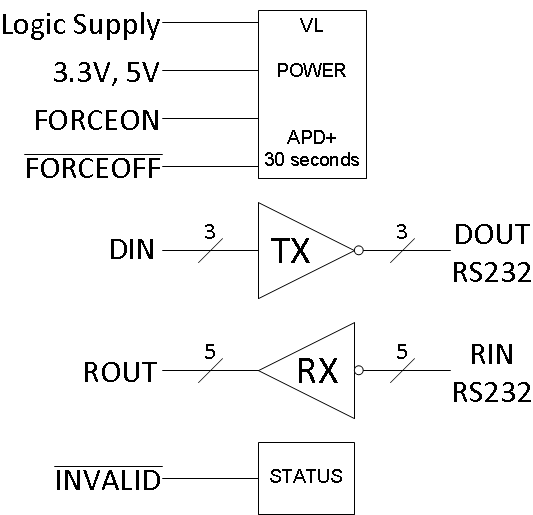
The TRS3253E is a three-driver and five-receiver RS-232 interface device, with split-supply pins for mixed-signal operations. All RS-232 inputs and outputs are protected to ±15 kV using the IEC 61000-4-2 Air-Gap Discharge method, ±8 kV using the IEC 61000-4-2 Contact Discharge method, and ±15 kV using the Human-Body Model. The charge pump requires only four small 0.1-μF capacitors for operation from a 3.3-V supply. The TRS3253E is capable of running at data rates up to 1000 kbps, while maintaining RS-232-compliant output levels. The TRS3253E is available in a space-saving VQFN package (4-mm × 4-mm RSM).
The TRS3253E has a unique VL pin that allows operation in mixed-logic voltage systems. Both driver input (DIN) and receiver output (ROUT) logic levels are pin programmable through the VL pin. This eliminates the need for additional voltage level shifter while interfacing with low-voltage microcontroller or UARTs.
Auto-powerdown plus can be disabled when FORCEON and FORCEOFF are high. With auto-powerdown plus enabled, the device activates automatically when a valid signal change is applied to any receiver or driver input. After 30 seconds of inactivity the device will automatically power down to save power.
INVALID is high (valid data) if any receiver input voltage is greater than 2.7 V or less than –2.7 V, or has been between –0.3 V and 0.3 V for less than 30 μs. INVALID is low (invalid data) if all receiver input voltages are between –0.3 V and 0.3 V for more than 30 μs. Refer to Figure 7 for receiver input levels.
8.2 Functional Block Diagram

8.3 Feature Description
8.3.1 Power
The power block increases, inverts, and regulates voltage at V+ and V– pins using a charge pump that requires four external capacitors. Logic voltage translation is controlled by voltage provided to VL pin. Auto-powerdown-plus feature is controlled by FORCEON and FORCEOFF inputs. See Table 1 and Table 2.
When TRS3253E is unpowered, it can be safely connected to an active remote RS232 device.
8.3.2 RS232 Driver
Three drivers interface standard logic level to RS232 levels. All DIN inputs must be valid high or low.
8.3.3 RS232 Receiver
Five receivers interface RS232 levels to standard logic levels. An open input will result in a high output on ROUT. Each RIN input includes an internal standard RS232 load.
8.3.4 RS232 Status
The INVALID output goes low when all RIN inputs are unpowered for more than 30 μs. The INVALID output goes high when any receiver has a valid input. The INVALID output is active when VL is powered irregardless of FORCEON and FORCEOFF inputs. See Table 3.
8.4 Device Functional Modes
Table 1. Each Driver(1)
| INPUTS | OUTPUT | DRIVER STATUS | |||
|---|---|---|---|---|---|
| DIN | FORCEON | FORCEOFF | TIME ELAPSED SINCE LAST RIN OR DIN TRANSITION |
DOUT | |
| X | X | L | X | Z | Powered off |
| L | H | H | X | H | Normal operation with auto-powerdown plus disabled |
| H | H | H | X | L | |
| L | L | H | <30 s | H | Normal operation with auto-powerdown plus enabled |
| H | L | H | <30 s | L | |
| L | L | H | >30 s | Z | Powered off by auto-powerdown plus feature |
| H | L | H | >30 s | Z | |
Table 2. Each Receiver(1)
| INPUTS | OUTPUT | RECEIVER STATUS | ||
|---|---|---|---|---|
| RIN | FORCEOFF | TIME ELAPSED SINCE LAST RIN OR DIN TRANSITION |
ROUT | |
| X | L | X | Z | Powered off |
| L | H | <30 s | H | Normal operation with auto-powerdown plus disabled/enabled |
| H | H | <30 s | L | |
| Open | H | <30 s | H | |
Table 3. INVALID(1)
| INPUTS | OUTPUT | |||
|---|---|---|---|---|
| RIN1 – RIN5 | FORCEON | FORCEOFF | TIME ELAPSED SINCE LAST RIN OR DIN TRANSITION |
INVALID |
| Any L or H | X | X | X | H |
| All Open | X | X | X | L |