SCDS311D January 2010 – October 2022 TS3A27518E-Q1
PRODUCTION DATA
- 1 Features
- 2 Applications
- 3 Description
- 4 Revision History
- 5 Pin Configuration and Functions
- 6 Specifications
- 7 Parameter Measurement Information
- 8 Detailed Description
- 9 Application and Implementation
- 10Power Supply Recommendations
- 11Layout
- 12Device and Documentation Support
- 13Mechanical, Packaging, and Orderable Information
Package Options
Mechanical Data (Package|Pins)
Thermal pad, mechanical data (Package|Pins)
- RTW|24
Orderable Information
3 Description
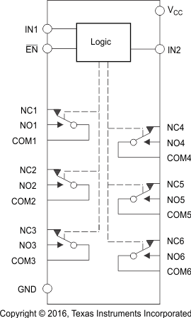
The TS3A27518E-Q1 is a 6-bit 1-of-2 multiplexer-demultiplexer designed to operate from 1.65 V to 3.6 V. This device can handle both digital and analog signals, and signals up to V+ can be transmitted in either direction. The TS3A27518E-Q1 has two control pins, each controlling three 1-of-2 muxes at the same time, and an enable pin that is used to put all outputs in high-impedance mode. The control pins are compatible with 1.8-V logic thresholds and are backward compatible with 2.5-V and 3.3-V logic thresholds as well.
The TS3A27518E-Q1 allows any SD, SDIO, and multimedia card host controllers to be expanded out to multiple cards or peripherals because the SDIO interface consists of 6-bits: CMD, CLK, and Data[0:3] signals. The TS3A27518E-Q1 has two control pins that give additional flexibility to the user, for example, the ability to mux two different audio-video signals in equipment such as an LCD television, an LCD monitor, or a notebook docking station.
| PART NUMBER | PACKAGE | BODY SIZE (NOM) |
|---|---|---|
| TS3A27518E-Q1 | RTW (WQFN, 24) | 4.00 mm × 4.00 mm |
| PW (TSSOP, 24) | 7.80 mm × 4.40 mm |
 Functional Block Diagram