SCDS339B January 2013 – April 2017 TS3A5223
PRODUCTION DATA.
- 1 Features
- 2 Applications
- 3 Description
- 4 Revision History
- 5 Pin Configuration and Functions
- 6 Specifications
- 7 Parameter Measurement Information
- 8 Detailed Description
- 9 Application and Implementation
- 10Power Supply Recommendations
- 11Layout
- 12Device and Documentation Support
- 13Mechanical, Packaging, and Orderable Information
Package Options
Mechanical Data (Package|Pins)
- RSW|10
Thermal pad, mechanical data (Package|Pins)
Orderable Information
7 Parameter Measurement Information
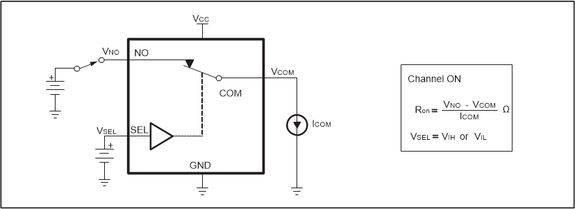 Figure 7. ON-State Resistance (RON)
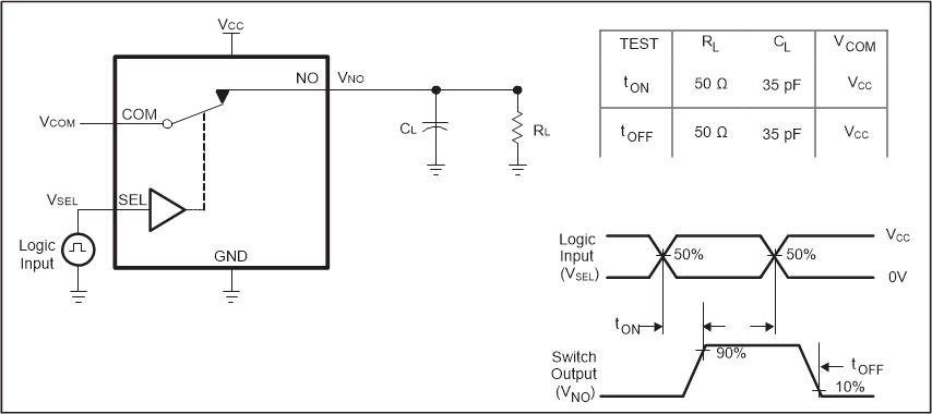 Figure 8. Turn-On (tON) and Turn-Off Time (tOFF)
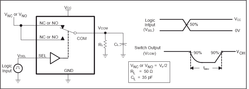 Figure 9. Break-Before-Make Time (tBBM)
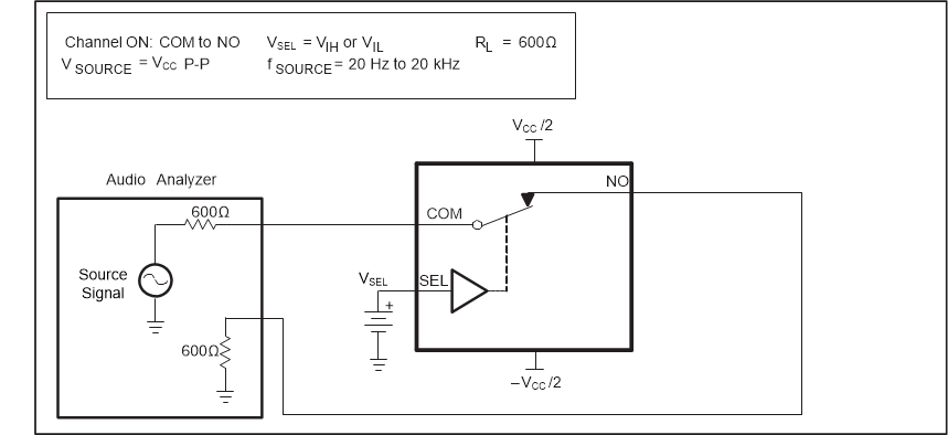 Figure 10. TOTAL HARMONIC DISTORTION (THD)
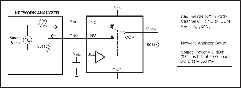 Figure 11. Crosstalk (XTALK)
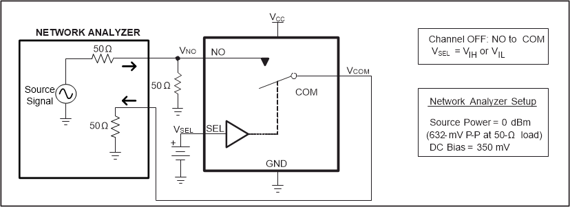 Figure 12. OFF Isolation (OISO)