SCDS324E August 2011 – Oct 2019 TS3DS10224
PRODUCTION DATA.
- 1 Features
- 2 Applications
- 3 Description
- 4 Revision History
- 5 Pin Configuration and Functions
-
6 Specifications
- 6.1 Absolute Maximum Ratings
- 6.2 ESD Ratings
- 6.3 Recommended Operating Conditions
- 6.4 Thermal Information
- 6.5 Electrical Characteristics: Differential 1:4 or 2‑Channel 1:2 Configurations
- 6.6 Electrical Characteristics: Fan-Out 1:2 Configurations
- 6.7 Switching Characteristics: Differential 1:4 or 2‑Channel 1:2 Configurations
- 6.8 Switching Characteristics: Fan-Out 1:2 Configurations
- 6.9 Dynamic Characteristics: Differential 1:4 or 2‑Channel 1:2 Configurations
- 6.10 Dynamic Characteristics: Fan-Out 1:2 Configurations
- 6.11 Typical Characteristics
- 7 Parameter Measurement Information
- 8 Detailed Description
- 9 Application and Implementation
- 10Power Supply Recommendations
- 11Layout
- 12Device and Documentation Support
- 13Mechanical, Packaging, and Orderable Information
Package Options
Refer to the PDF data sheet for device specific package drawings
Mechanical Data (Package|Pins)
- RUK|20
Thermal pad, mechanical data (Package|Pins)
- RUK|20
Orderable Information
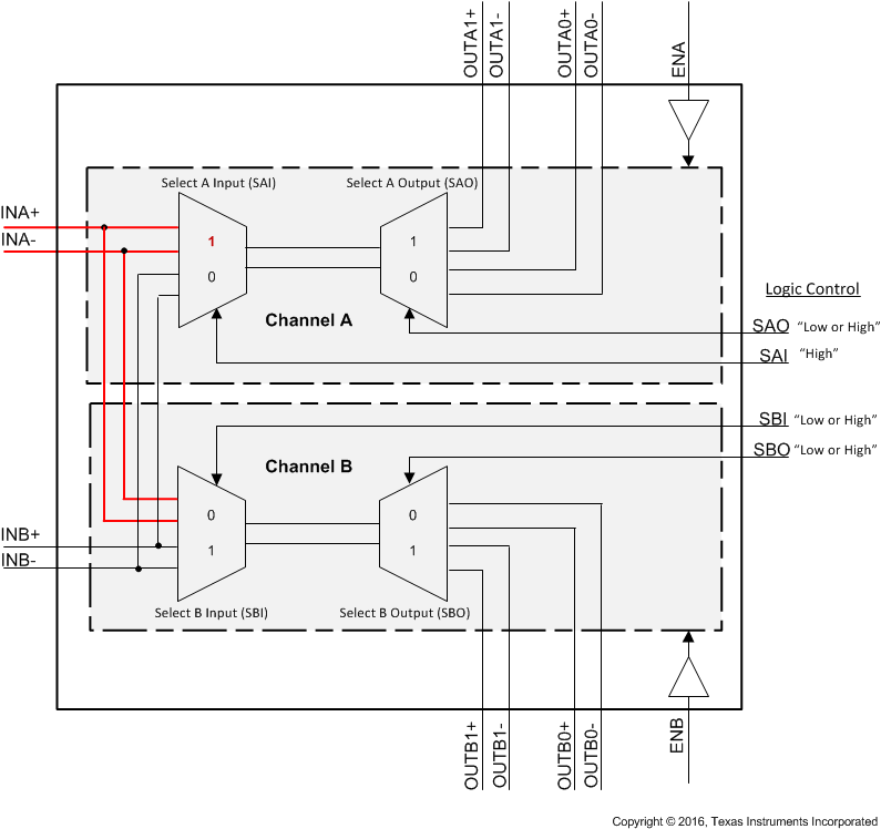
8.4.4 1-Channel 1:4 Mux
The TS3DS10224 can be configured as differential 1-channel 1:4 mux.
The truth table below shows that the inputs INA can be routed to 4 different places. This is accomplished by setting the Select A Input (SAI) and Select B Input (SBI) HIGH and selecting an output by toggling the Select A Output (SAO) and Select B Output (SBO) pins.
Unused pins INB+ and INB– must be left floating in this configuration.
Table 4. 1-Channel 1:4 Mux Function Table
| LOGIC CONTROL SETTINGS | SIGNAL ROUTING | ||||
|---|---|---|---|---|---|
| SAI | SBI | SAO | SBO | INA | INB |
| 1 | 1 | 0 | — | OUTA0 | — |
| 1 | 1 | 1 | — | OUTA1 | — |
| 0 | 0 | — | 0 | OUTB0 | — |
| 0 | 0 | — | 1 | OUTB1 | — |
 Figure 16. 1-Channel 1:4 Mux Functional Block Diagram