SCDS430A December 2020 – May 2021 TS3DV642-Q1
PRODUCTION DATA
- 1 Features
- 2 Applications
- 3 Description
- 4 Revision History
- 5 Pin Configuration and Functions
- 6 Specifications
- 7 Parameter Measurement Information
- 8 Detailed Description
- 9 Application and Implementation
- 10Power Supply Recommendations
- 11Layout
- 12Device and Documentation Support
- 13Mechanical, Packaging, and Orderable Information
Package Options
Refer to the PDF data sheet for device specific package drawings
Mechanical Data (Package|Pins)
- RUA|42
Thermal pad, mechanical data (Package|Pins)
Orderable Information
9.2.3 Application Curves
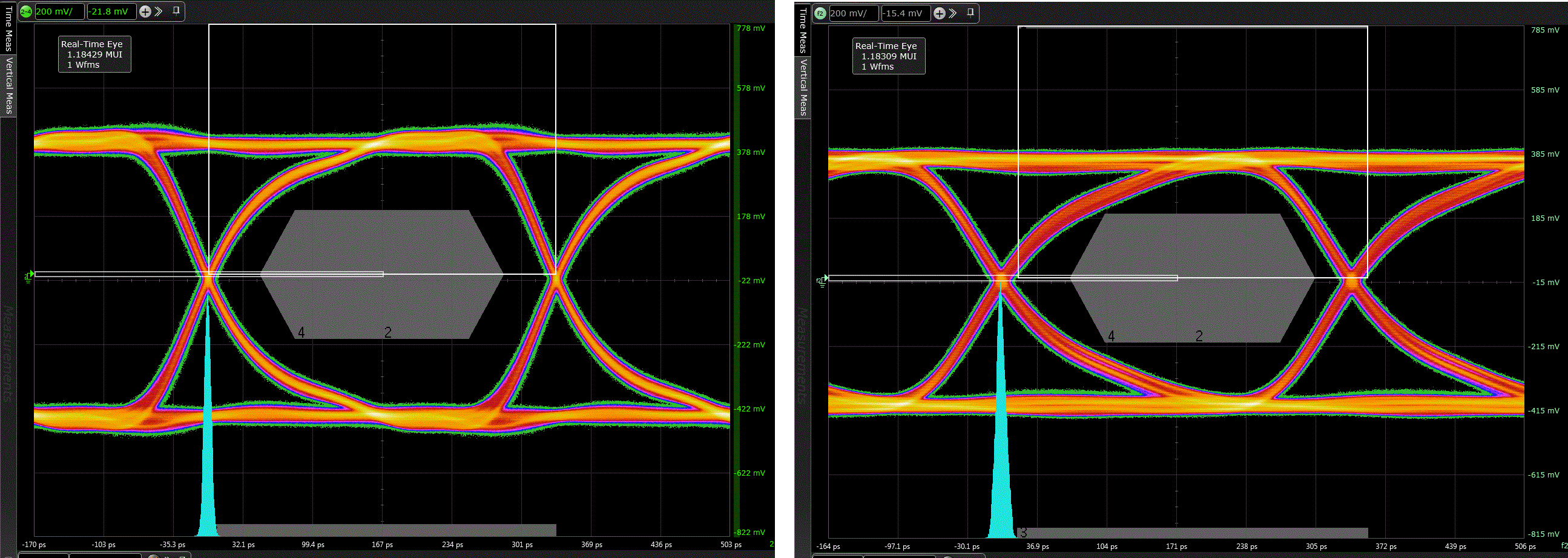
An HDMI connector functioning as a source is subject to HDMI source compliance test. This section provides application curves related to HDMI 1.4 and 2.0 source compliance for jitter and eye mask respectively.
Figure 9-2 shows HDMI 1.4 compliance jitter performance at 3.0 Gbps data rate. For brevity only one of the three data channels and Port A illustrated. Other channels have similar performances. As illustration shows the TS3DV642-Q1 adds minimal jitter to the link - 89 mTbit through mux vs 73 mTbit without mux.
 Figure 9-2 HDMI 1.4 compliance at 3.0 Gbps -
jitter performance. Left: with no DUT in the path. Right: TS3DV642-Q1 in the path
Figure 9-2 HDMI 1.4 compliance at 3.0 Gbps -
jitter performance. Left: with no DUT in the path. Right: TS3DV642-Q1 in the pathFigure 9-3 shows HDMI 2.0 eye mask performance at 6.0 Gbps data rate. For brevity only one of the three data channels and Port A is illustrated. Eye masks are for worst case positive skew. Other channels, and cases have similar performances.
 Figure 9-3 HDMI 2.0 compliance at 6.0 Gbps - eye
mask at TP2_EQ. Left - with no DUT in the path. Right - TS3DV642-Q1 in the path