SCDS176B SEPTEMBER   2004  – October 2019 TS3L110

PRODUCTION DATA.  

  1. Features
  2. Applications
  3. Description
    1.     Logic Diagram (Positive Logic)
  4. Revision History
  5. Pin Configuration and Functions
    1.     Pin Functions
  6. Specifications
    1. 6.1 Absolute Maximum Ratings
    2. 6.2 ESD Ratings
    3. 6.3 Recommended Operating Conditions
    4. 6.4 Thermal Information
    5. 6.5 Electrical Characteristics
    6. 6.6 Switching Characteristics
    7. 6.7 Dynamic Characteristics
    8. 6.8 Typical Characteristics
  7. Parameter Measurement Information
  8. Detailed Description
    1. 8.1 Overview
    2. 8.2 Functional Block Diagram
    3. 8.3 Feature Description
    4. 8.4 Device Functional Modes
  9. Application and Implementation
    1. 9.1 Application Information
    2. 9.2 Typical Application
      1. 9.2.1 Design Requirements
      2. 9.2.2 Detailed Design Procedure
      3. 9.2.3 Application Curves
  10. 10Power Supply Recommendations
  11. 11Layout
    1. 11.1 Layout Guidelines
    2. 11.2 Layout Example
  12. 12Device and Documentation Support
    1. 12.1 Receiving Notification of Documentation Updates
    2. 12.2 Community Resources
    3. 12.3 Trademarks
    4. 12.4 Electrostatic Discharge Caution
    5. 12.5 Glossary
  13. 13Mechanical, Packaging, and Orderable Information

Package Options

Refer to the PDF data sheet for device specific package drawings

Mechanical Data (Package|Pins)
  • PW|16
  • DBQ|16
  • RGY|16
  • D|16
  • DGV|16
Thermal pad, mechanical data (Package|Pins)
Orderable Information

Parameter Measurement Information

TS3L110 tstcnd1_cds176.gif
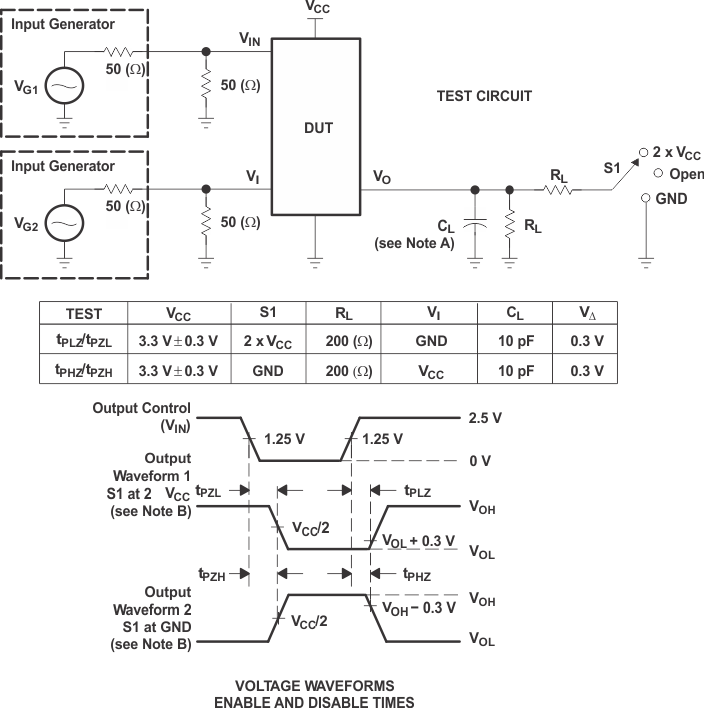
CL includes probe and jig capacitance.
Waveform 1 is for an output with internal conditions such that the output is low. Waveform 2 is for an output with internal conditions such that the output is high, except when disabled by the output control.
All input pulses are supplied by generators having the following characteristics: PRR ≤ 10 MHz, ZO = 50 Ω, tr ≤ 2.5 ns, tf ≤ 2.5 ns.
The outputs are measured one at a time, with one transition per measurement.
tPLZ and tPHZ are the same as tdis.
tPLZ and tPHH are the same as ten.
Figure 5. Test Circuit and Voltage Waveforms
TS3L110 tstcnd2_cds176.gif
CL includes probe and jig capacitance.
Switch is ON during the measurement of tsk(p), that is, voltage at E = 0 and S = VCC or GND.
Figure 6. Test Circuit and Voltage Waveforms
TS3L110 tstcir1_cds176.gif
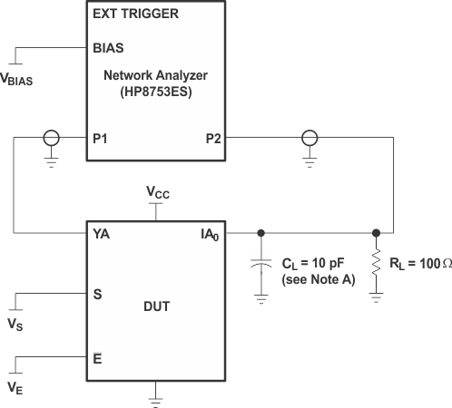
CL includes probe and jig capacitance.
Figure 7. Test Circuit for Frequency Response (BW)

Frequency response is measured at the output of the ON channel. For example, when VS = 0, VE = 0, and YA is the input, the output is measured at IA0. All unused analog I/O ports are left open.

HP8753ES Setup

  • Average = 4
  • RBW = 3 kHz
  • VBIAS = 0.35 V
  • ST = 2 s
  • P1 = 0 dBM

TS3L110 tstcir2_cds176.gif
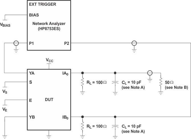
CL includes probe and jig capacitance.
A 50-Ω termination resistor is needed to match the loading of the network analyzer
Figure 8. Test Circuit for Crosstalk (XTALK)

Crosstalk is measured at the output of the nonadjacent ON channel. For example, when VS = 0, VE = 0, and YA is the input, the output is measured at IB0. All unused analog input (Y) ports are connected to GND, and output (I) ports are connected to GND through 50-Ω pulldown resistors.

HP8753ES Setup

  • Average = 4
  • RBW = 3 kHz
  • VBIAS = 0.35 V
  • ST = 2 s
  • P1 = 0 dBM

TS3L110 tstcir3_cds176.gif
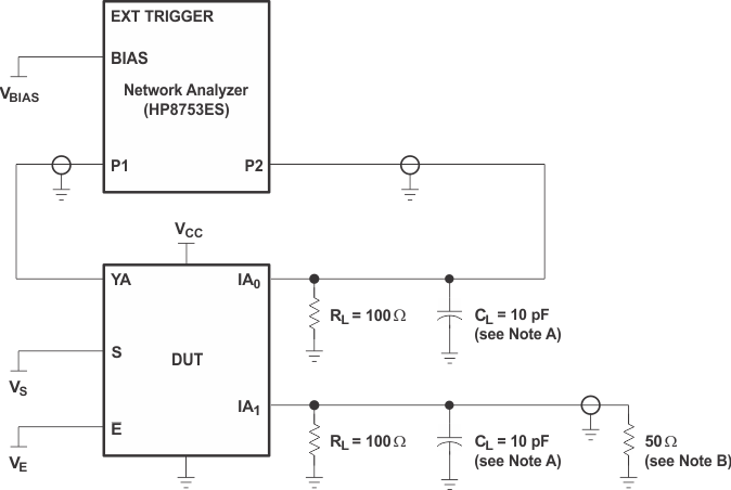
CL includes probe and jig capacitance.
A 50-Ω termination resistor is needed to match the loading of the network analyzer
Figure 9. Test Circuit for OFF Isolation (OIRR)

OFF isolation is measured at the output of the OFF channel. For example, when VS = VCC, VE = 0, and YA is the input, the output is measured at IA0. All unused analog input (Y) ports are left open, and output (I) ports are connected to GND through 50-Ω pulldown resistors.

HP8753FS Setup

  • Average = 4
  • RBW = 3 kHz
  • VBIAS = 0.35 V
  • ST = 2 s
  • P1 = 0 dBM