SCDS277C November 2008 – October 2024 TS3USB221A
PRODUCTION DATA
- 1
- 1 Features
- 2 Applications
- 3 Description
- 4 Pin Configuration and Functions
-
5 Specifications
- 5.1 Absolute Maximum Ratings
- 5.2 ESD Ratings
- 5.3 Recommended Operating Conditions
- 5.4 Thermal Information
- 5.5 Electrical Characteristics
- 5.6 Dynamic Electrical Characteristics, VCC = 3.3V ±10%
- 5.7 Dynamic Electrical Characteristics, VCC = 2.5V ±10%
- 5.8 Switching Characteristics, VCC = 3.3V ±10%
- 5.9 Switching Characteristics, VCC = 2.5V ±10%
- 5.10 Typical Characteristics
- 6 Parameter Measurement Information
- 7 Detailed Description
- 8 Application and Implementation
- 9 Device and Documentation Support
- 10Revision History
- 11Mechanical, Packaging, and Orderable Information
Package Options
Mechanical Data (Package|Pins)
- RSE|10
Thermal pad, mechanical data (Package|Pins)
Orderable Information
8.4.1 Layout Guidelines
Place supply bypass capacitors as close to VCC pin as possible and avoid placing the bypass caps near the D+/D– traces.
Make sure the high speed D+/D– trace lengths match and are no more than 4 inches; otherwise, the eye diagram performance can degrade. A high-speed USB connection is made through a shielded, twisted pair cable with a differential characteristic impedance. In layout, make sure the impedance of D+ and D– traces match the cable characteristic differential impedance for optimal performance.
Route the high-speed USB signals using a minimum of vias and corners to reduce signal reflections and impedance changes. When a via must be used, increase the clearance size around the via to minimize the capacitance. Each via introduces discontinuities in the transmission line of the signal and increases the chance of picking up interference from the other layers of the board. Be careful when designing test points on twisted pair lines; through-hole pins are not recommended.
When it becomes necessary to turn 90°, use two 45° turns or an arc instead of making a single 90° turn. This reduces reflections on the signal traces by minimizing impedance discontinuities.
Do not route USB traces under or near crystals, oscillators, clock signal generators, switching regulators, mounting holes, magnetic devices or ICs that use or duplicate clock signals.
Avoid stubs on the high-speed USB signals because stubs cause signal reflections. If a stub is unavoidable, keep the stub less than 200mm.
Route all high-speed USB signal traces over continuous planes (VCC or GND), with no interruptions.
Avoid crossing over anti-etch, commonly found with plane splits.
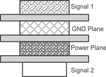
Due to high frequencies associated with the USB, a printed circuit board with at least four layers is recommended; two signal layers separated by a ground and power layer as shown in Figure 8-5.
 Figure 8-5 Four-Layer Board Stack-Up
Make sure the majority of signal traces run on a single layer, preferably Signal 1. Make sure the GND plane, which is solid with no cuts, is immediately next to this layer. Avoid running signal traces across a split in the ground or power plane. When running across split planes is unavoidable, sufficient decoupling must be used. Minimizing the number of signal vias reduces EMI by reducing inductance at high frequencies.