SCDS348D September 2013 – August 2024 TS3USB3031
PRODUCTION DATA
- 1
- 1 Features
- 2 Applications
- 3 Description
- 4 Pin Configuration and Functions
- 5 Specifications
- Parameter Measurement Information
- 6 Detailed Description
- 7 Application and Implementation
- 8 Device and Documentation Support
- 9 Revision History
- 10Mechanical, Packaging, and Orderable Information
Package Options
Mechanical Data (Package|Pins)
- RMG|12
Thermal pad, mechanical data (Package|Pins)
Orderable Information
3 Description
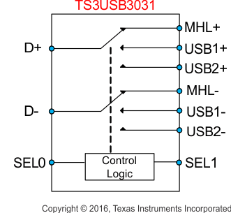
The TS3USB3031 device is a 2-channel, 1:3 multiplexer that includes a high-speed Mobile High-Definition Link (MHL), Mobility Display Port (MyDP) switch, and USB 2.0 High-Speed (480Mbps) switches in the same package. These configurations allow the system designer to save board space and eliminate multiple connectors buy using a common USB or Mico-USB connector for MHL/MyDP signals and two sets of USB data. The MHL/MyDP path supports the latest MHL Rev. 3.0 specification.
The TS3USB3031 has a VCC range of 2.5V to 4.3V and supports overvoltage tolerance (OVT) feature, which allows the I/O pins to withstand overvoltage conditions (up to 5.5V). The power-off protection feature forces all I/O pins to be in high impedance mode when power is not present, allowing full isolation of the signals lines under such condition without excessive leakage current. The select pins of TS3USB3031 are compatible with 1.8V control voltage, allowing them to be directly interfaced with the General Purpose I/O (GPIO) from a mobile processor with out needing additional voltage level shifting circuitry.
The TS3USB3031 is available in a small 1.8mm × 1.8mm 12-pin VQFN package designed for mobile applications.
 Switch Diagram