SCDS328C October 2011 – August 2015 TS3USBA225
PRODUCTION DATA.
- 1 Features
- 2 Applications
- 3 Description
- 4 Revision History
- 5 Pin Configuration and Functions
- 6 Specifications
- 7 Detailed Description
- 8 Application and Implementation
- 9 Power Supply Recommendations
- 10Layout
- 11Device and Documentation Support
- 12Mechanical, Packaging, and Orderable Information
Package Options
Mechanical Data (Package|Pins)
- RUT|12
Thermal pad, mechanical data (Package|Pins)
Orderable Information
8 Application and Implementation
NOTE
Information in the following applications sections is not part of the TI component specification, and TI does not warrant its accuracy or completeness. TI’s customers are responsible for determining suitability of components for their purposes. Customers should validate and test their design implementation to confirm system functionality.
8.1 Application Information
The TS3USBA225 is typically used to route signals from one USB connector to multiple signal paths in a system including an analog audio/negative signal path. All signal paths through the device are unbuffered bidirectional path which can represented by perfect 0 Ω impedance wire in an ideal case. All signal paths can handle USB 2.0 signals but the L and R paths are the only paths that can support a negative signal.
8.2 Typical Application
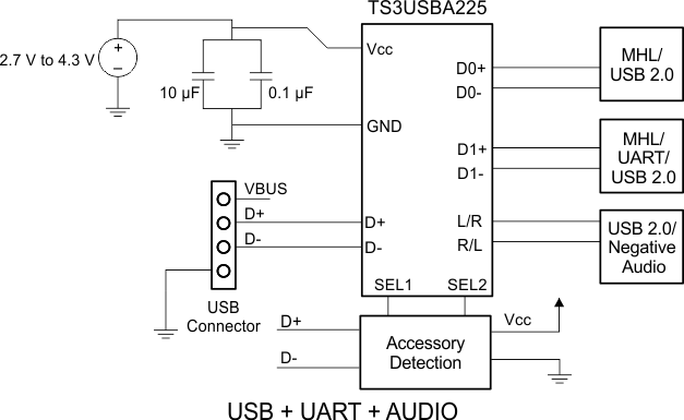 Figure 13. Application Block Diagram
8.2.1 Design Requirements
Design requirements of the USB 1.0, 1.1, and 2.0 standards should be followed.
TI recommends that the digital control pins SEL1 and SEL2 be pulled up to VCC or down to GND to avoid undesired switch positions that could result from the floating logic pin.
8.2.2 Detailed Design Procedure
The TS3USB221 can be properly operated without any external components. However, it is recommended that unused pins should be connected to ground through a 50 Ω resistor to prevent signal reflections back into the device.
8.2.3 Application Curves
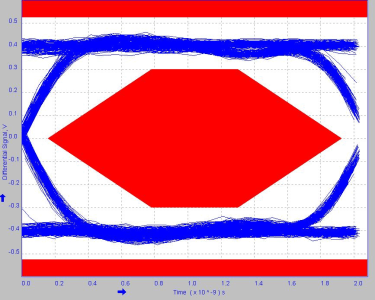 Figure 14. Eye Pattern: 480-Mbps USB 2.0 Eye Pattern (No Switch)
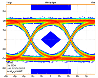 Figure 18. MHL Eye Pattern: 720p 60 fps, 1080i 30fps (No Switch)
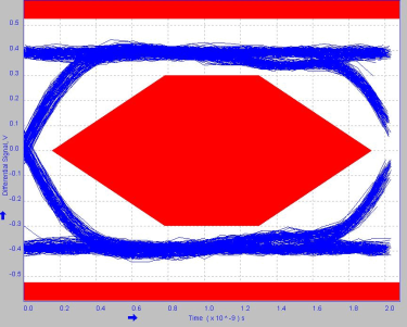 Figure 15. Eye Pattern: 480-Mbps USB 2.0 Eye Pattern for USB Switch
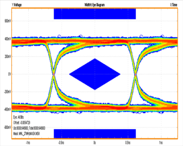 Figure 17. MHL Eye Pattern: 480p 60 fps (With Switch)
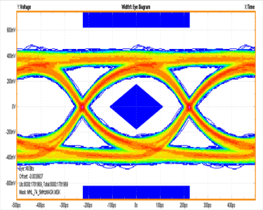 Figure 19. MHL Eye Pattern: 720p 60 fps, 1080i 30fps (With Switch)
