SLLSF73C February 2018 – September 2019 TS3USBCA4
PRODUCTION DATA.
- 1 Features
- 2 Applications
- 3 Description
- 4 Revision History
- 5 Pin Configuration and Functions
-
6 Specifications
- 6.1 Absolute Maximum Ratings
- 6.2 ESD Ratings
- 6.3 Recommended Operating Conditions
- 6.4 Thermal Information
- 6.5 Electrical Characteristics (3 V ≤ VCC ≤ 3.6 V)
- 6.6 Electrical Characteristics (2.4 V ≤ VCC ≤ 5.5 V)
- 6.7 Switching Characteristics (2.4 V ≤ VCC ≤ 5.5 V)
- 6.8 Timing Requirements (3 V ≤ VCC ≤ 3.6 V)
- 6.9 Timing Requirements (2.4 V ≤ VCC ≤ 5.5 V)
- 6.10 Timing Diagrams
- 6.11 Typical Characteristics
- 7 Parameter Measurement Information
-
8 Detailed Description
- 8.1 Overview
- 8.2 Functional Block Diagram
- 8.3 Feature Description
- 8.4 Device Functional Modes
- 8.5 Programming
- 8.6 Register Maps
- 9 Application and Implementation
- 10Power Supply Recommendations
- 11Layout
- 12Device and Documentation Support
- 13Mechanical, Packaging, and Orderable Information
Package Options
Mechanical Data (Package|Pins)
- RSV|16
Thermal pad, mechanical data (Package|Pins)
Orderable Information
9.2 Typical Application
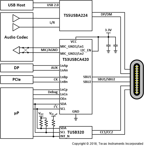
Figure 21 shows the typical application of TS3USBCA420 in I2C-configuration mode from a 3.3-V supply. The I2C slave address is set to ADDR1. VIO_uP is the supply for the micro-processor IOs.
 Figure 21. Application of TS3USBCA420 in I2C-Configuration Mode
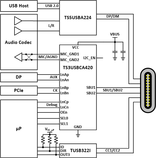
 Figure 22 shows the typical application of TS3USBCA420 in pin-configuration mode from VBUS. VIO_uP is the supply for the micro-processor IOs.
 Figure 22. Application of TS3USBCA420 in Pin-Configuration Mode
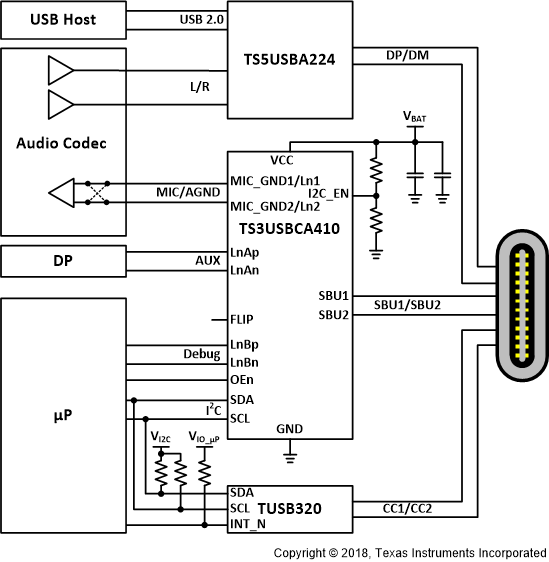
 Figure 21 shows the typical application of TS3USBCA410 in I2C-configuration mode from VBAT. The I2C slave address is set to ADDR0. VIO_uP is the supply for the micro-processor IOs.
 Figure 23. Application of TS3USBCA410 in I2C-Configuration Mode
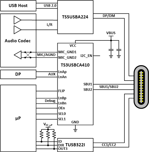
 Figure 22 shows the typical application of TS3USBCA410 in pin-configuration mode from VBUS. VIO_uP is the supply for the micro-processor IOs.
 Figure 24. Application of TS3USBCA410 in Pin-Configuration Mode