SCDS252B July 2007 – June 2021 TS5A23157-Q1
PRODUCTION DATA
- 1 Features
- 2 Applications
- 3 Description
- 4 Revision History
- 5 Pin Configurations and Functions
- 6 Specifications
- 7 Parameter Description
- 8 Parameter Measurement Information
- 9 Function and Summary of Characteristics
- 10Detailed Description
- 11Application and Implementation
- 12Power Supply Recommendations
- 13Layout
- 14Device and Documentation Support
- 15Mechanical, Packaging, and Orderable Information
Package Options
Mechanical Data (Package|Pins)
- DGS|10
Thermal pad, mechanical data (Package|Pins)
Orderable Information
13.1 Layout Guidelines
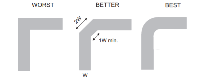
When a PCB trace turns a corner at a 90° angle, a reflection can occur. A reflection occurs primarily because of the change of width of the trace. At the apex of the turn, the trace width increases to 1.414 times the width. This increase upsets the transmission-line characteristics, especially the distributed capacitance and self–inductance of the trace which results in the reflection. Not all PCB traces can be straight and therefore some traces must turn corners.The figure below shows progressively better techniques of rounding corners. Only the last example (BEST) maintains constant trace width and minimizes reflections.
 Figure 13-1 Trace Guidelines for
TS5A23157-Q1
Figure 13-1 Trace Guidelines for
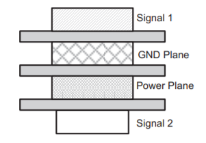
TS5A23157-Q1Route the high-speed signals using a minimum of vias and corners which reduces signal reflections and impedance changes. When a via must be used, increase the clearance size around it to minimize its capacitance. Each via introduces discontinuities in the signal’s transmission line and increases the chance of picking up interference from the other layers of the board. Be careful when designing test points, throughhole pins are not recommended at high frequencies. Do not route high speed signal traces under or near crystals, oscillators, clock signal generators, switching regulators, mounting holes, magnetic devices or ICs that use or duplicate clock signals. Avoid stubs on the high-speed signals traces because they cause signal reflections. Route all high-speed signal traces over continuous GND planes, with no interruptions. Avoid crossing over anti-etch, commonly found with plane splits. When working with high frequencies, a printed circuit board with at least four layers is recommended; two signal layers separated by a ground and power layer as shown below.
 Figure 13-2 Layer Stack Example for
TS5A23157-Q1 device.