SCDS201H AUGUST 2005 – February 2015 TS5A23159
PRODUCTION DATA.
- 1 Features
- 2 Applications
- 3 Description
- 4 Revision History
- 5 Pin Configuration and Functions
-
6 Specifications
- 6.1 Absolute Maximum Ratings
- 6.2 ESD Ratings
- 6.3 Recommended Operating Conditions
- 6.4 Thermal Information
- 6.5 Electrical Characteristics for 5-V Supply
- 6.6 Electrical Characteristics for 3.3-V Supply
- 6.7 Electrical Characteristics for 2.5-V Supply
- 6.8 Electrical Characteristics for 1.8-V Supply
- 6.9 Typical Characteristics
- 7 Parameter Measurement Information
- 8 Detailed Description
- 9 Application and Implementation
- 10Power Supply Recommendations
- 11Layout
- 12Device and Documentation Support
- 13Mechanical, Packaging, and Orderable Information
Package Options
Refer to the PDF data sheet for device specific package drawings
Mechanical Data (Package|Pins)
- RSE|10
- DGS|10
Thermal pad, mechanical data (Package|Pins)
Orderable Information
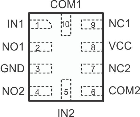
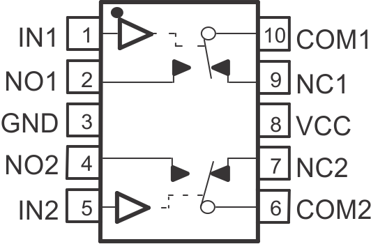
5 Pin Configuration and Functions
RSE Package
10-Pin UQFN
Top View

DGS Package
10-Pin VSSOP
Top View

Pin Functions
| PIN | I/O | DESCRIPTION | |
|---|---|---|---|
| NO. | NAME | ||
| 1 | IN1 | I | Digital control to connect COM to NO or NC |
| 2 | NO1 | I/O | Normally open |
| 3 | GND | — | Ground |
| 4 | NO2 | I/O | Normally open |
| 5 | IN2 | I | Digital control to connect COM to NO or NC |
| 6 | COM2 | I/O | Common |
| 7 | NC2 | I/O | Normally closed |
| 8 | VCC | — | Power supply |
| 9 | NC1 | I/O | Normally closed |
| 10 | COM1 | I/O | Common |