SCDS196J May 2005 – September 2019 TS5A23166
PRODUCTION DATA.
- 1 Features
- 2 Applications
- 3 Description
- 4 Revision History
- 5 Pin Configuration and Functions
-
6 Specifications
- 6.1 Absolute Maximum Ratings
- 6.2 ESD Ratings
- 6.3 Recommended Operating Conditions
- 6.4 Thermal Information
- 6.5 Electrical Characteristics: 5-V Supply
- 6.6 Electrical Characteristics: 3.3-V Supply
- 6.7 Electrical Characteristics: 2.5-V Supply
- 6.8 Electrical Characteristics: 1.8-V Supply
- 6.9 Switching Characteristics: 5-V Supply
- 6.10 Switching Characteristics: 3.3-V Supply
- 6.11 Switching Characteristics: 2.5-V Supply
- 6.12 Switching Characteristics: 1.8-V Supply
- 6.13 Typical Characteristics
- 7 Parameter Measurement Information
- 8 Detailed Description
- 9 Application and Implementation
- 10Power Supply Recommendations
- 11Layout
- 12Device and Documentation Support
- 13Mechanical, Packaging, and Orderable Information
Package Options
Mechanical Data (Package|Pins)
Thermal pad, mechanical data (Package|Pins)
Orderable Information
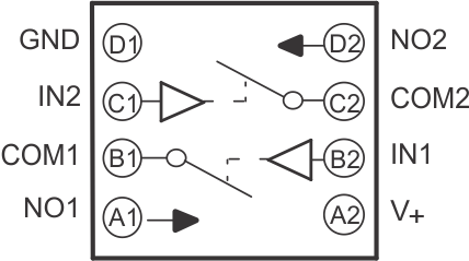
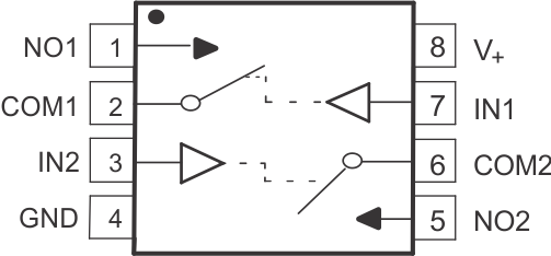
5 Pin Configuration and Functions
YZT or YZP Package
8-Pin DSBGA
Bottom View

Pin Functions
| PIN | TYPE | DESCRIPTION | ||
|---|---|---|---|---|
| NAME | TSSOP NO. | DSBGA NO. | ||
| COM1 | 2 | B1 | I/O | Common port for switch 1 |
| COM2 | 6 | C2 | I/O | Common port for switch 2 |
| GND | 4 | D1 | GND | Ground |
| IN1 | 7 | B2 | I | Active-high control pin connecting NO1 to COM1. |
| IN2 | 3 | C1 | I | Active-high control pin connecting NO2 to COM2. |
| NO1 | 1 | A1 | I/O | Normally open switch path 1 |
| NO2 | 5 | D2 | I/O | Normally open switch path 2 |
| V+ | 8 | A2 | PWR | Power supply pin |
