SLLS783C May   2009  – March 2016 TSB81BA3E

PRODUCTION DATA.  

  1. Features
  2. Description
  3. Revision History
  4. Description Continued
  5. Pin Configuration and Function
  6. Electrical Specfications
    1. 6.1 Absolute Maximum Ratings
    2. 6.2 Thermal Information
    3. 6.3 Recommended Operating Conditions
    4. 6.4 Electrical Characteristics, Driver
    5. 6.5 Electrical Characteristics, Receiver
    6. 6.6 Electrical Characteristics, Device
    7. 6.7 Switching Characteristics
  7. Parameter Measurement Information
  8. Detailed Description
    1. 8.1 Overview
    2. 8.2 Functional Block Diagram
    3. 8.3 Feature Description
      1. 8.3.1 TTL Input Data
      2. 8.3.2 LVDS Output Data
    4. 8.4 Device Functional Modes
      1. 8.4.1 Input Clock Edge
      2. 8.4.2 Low Power Mode
      3. 8.4.3 1394b Port Interface Considerations
    5. 8.5 Programming
      1. 8.5.1 Power-Class
    6. 8.6 Register Maps
      1. 8.6.1 Internal Register Configuration
  9. Application and Implementation
    1. 9.1 Application Information
    2. 9.2 Typical Application
      1. 9.2.1 Design Requirements
      2. 9.2.2 Detailed Design Procedure
        1. 9.2.2.1 Port Termination for a 1394 Bilingual Port
        2. 9.2.2.2 PHY-LINK Interface
  10. 10Power Supply Recommendations
  11. 11Layout
    1. 11.1 Layout Guidelines
      1. 11.1.1 Board Stackup
      2. 11.1.2 Digital and Analog Partitioning
      3. 11.1.3 Image Planes
      4. 11.1.4 Parts Placement
      5. 11.1.5 Decoupling Capacitors
      6. 11.1.6 3W Rule for SCLK
  12. 12Device and Documentation Support
    1. 12.1 Device Support
    2. 12.2 Related Links
    3. 12.3 Community Resources
    4. 12.4 Trademarks
    5. 12.5 Electrostatic Discharge Caution
    6. 12.6 Glossary
  13. 13Mechanical, Packaging, and Orderable Information
    1. 13.1 Designing With PowerPAD Devices (PFP Package Only)

Package Options

Mechanical Data (Package|Pins)
Thermal pad, mechanical data (Package|Pins)
Orderable Information

7 Parameter Measurement Information
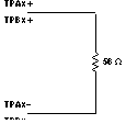
TSB81BA3E fig1_lls782.gif Figure 1. Test Load Diagram
TSB81BA3E fig3_lls782.gif Figure 3. Dx and CTLx Output Delay Relative to xCLK Waveforms
TSB81BA3E fig2_lls782.gif Figure 2. Dx, CTLx, LREQ Input Setup and Hold Time Waveforms