SBAS545A September 2011 – December 2016 TSC2007-Q1
PRODUCTION DATA.
- 1 Features
- 2 Applications
- 3 Description
- 4 Revision History
- 5 Pin Configuration and Functions
-
6 Specifications
- 6.1 Absolute Maximum Ratings
- 6.2 ESD Ratings
- 6.3 Recommended Operating Conditions
- 6.4 Thermal Information
- 6.5 Electrical Characteristics
- 6.6 Timing Requirements: Standard Mode (SCL = 100 kHz)
- 6.7 Timing Requirements: Fast Mode (SCL = 400 kHz)
- 6.8 Timing Requirements: High-Speed Mode (SCL = 1.7 MHz)
- 6.9 Timing Requirements: High-Speed Mode (SCL = 3.4 MHz)
- 6.10 Typical Characteristics
- 7 Detailed Description
- 8 Application and Implementation
- 9 Power Supply Recommendations
- 10Layout
- 11Device and Documentation Support
- 12Mechanical, Packaging, and Orderable Information
Package Options
Mechanical Data (Package|Pins)
- PW|16
Thermal pad, mechanical data (Package|Pins)
Orderable Information
7 Detailed Description
7.1 Overview
The TSC2007-Q1 is an analog interface circuit for a human interface touch screen devices. All peripheral functions are controlled through the command byte and onboard state machines. The TSC2007-Q1 features include:
- Very low-power touch screen controller
- Very small onboard footprint
- Relieves host from tedious routine tasks by preprocessing, thus saving resources for more critical tasks
- Ability to work on very low supply voltage
- Minimal connection interface allows easy isolation and reduces the number of dedicated I/O pins required
- Miniature, yet complete; requires no external supporting components
- Enhanced electrostatic discharge (ESD) protection
The TSC2007-Q1 consists of the following blocks (see Functional Block Diagram):
- Touch Screen Sensor Interface
- Auxiliary Input (AUX)
- Temperature Sensor
- Acquisition Activity Preprocessing
- Internal Conversion Clock
- I2C Interface
Communication with the TSC2007-Q1 is done through an I2C serial interface. The TSC2007-Q1 is an I2C slave device; therefore, data are shifted into or out of the TSC2007-Q1 under control of the host microprocessor, which also provides the serial data clock.
Control of the TSC2007-Q1 and its functions is accomplished by writing to the command register of an internal state machine. A simple command protocol compatible with I2C is used to address this register.
7.2 Functional Block Diagram

7.3 Feature Description
7.3.1 Touch Screen Operation
A resistive touch screen operates by applying a voltage across a resistor network and measuring the change in resistance at a given point on the matrix where the screen is touched by an input (stylus, pen, or finger). The change in the resistance ratio marks the location on the touch screen.
The TSC2007-Q1 supports resistive 4-wire configurations, as shown in Figure 35. The circuit determines location in two coordinate pair dimensions, although a third dimension can be added for measuring pressure.
7.3.2 Internal Temperature Sensor
In some applications, such as battery recharging, an ambient temperature measurement is required. The temperature measurement technique used in the TSC2007-Q1 relies on the characteristics of a semiconductor junction operating at a fixed current level. The forward diode voltage (VBE) has a well-defined characteristic versus temperature. The ambient temperature can be predicted in applications by knowing the 25°C value of the VBE voltage and then monitoring the delta of that voltage as the temperature changes.
The TSC2007-Q1 offers two modes of temperature measurement. The first mode requires calibration at a known temperature, but only requires a single reading to predict the ambient temperature. The TEMP1 diode, shown in Figure 19, is used during this measurement cycle. This voltage is typically 580 mV at 25°C with a 10-µA current. The absolute value of this diode voltage can vary by a few millivolts; the temperature coefficient (TC) of this voltage is very consistent at –2.1 mV/°C. During the final test of the end product, the diode voltage would be stored at a known room temperature, in system memory, for calibration purposes by the user. The result is an equivalent temperature measurement resolution of 0.35°C/LSB (1 LSB = 732 µV with VREF = 3 V).
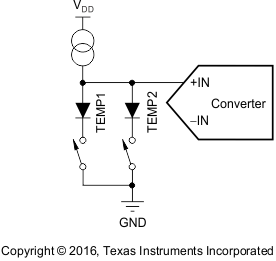 Figure 19. Functional Block Diagram of Temperature Measurement Mode
The second mode does not require a test temperature calibration, but uses a two-measurement (differential) method to eliminate the need for absolute temperature calibration and for achieving 2°C/LSB accuracy. This mode requires a second conversion of the voltage across the TEMP2 diode with a resistance 91 times larger than the TEMP1 diode. The voltage difference between the first (TEMP1) and second (TEMP2) conversion is represented by:

where
- N = the resistance ratio = 91.
- k = Boltzmann's constant = 1.3807 × 10⁻²³ J/K (joules per kelvins).
- q = the electron charge = 1.6022 × 10⁻¹⁹ C (coulombs).
- T = the temperature in kelvins (K).
This method can provide a much improved absolute temperature measurement, but a lower resolution of 1.6°C/LSB. Equation 2 solves for T:

where
- ΔV = VBE (TEMP2) – VBE(TEMP1) (in mV)
∴ T = 2.573 × ΔV (in K)
or T = 2.573 × ΔV – 273 (in °C)
Temperature 1 and temperature 2 measurements have the same timing as the other data acquisition cycles shown in Figure 32 and Figure 33.
7.3.3 Analog-to-Digital Converter
Figure 20 shows the analog inputs of the TSC2007-Q1. The analog inputs (X, Y, and Z touch panel coordinates, chip temperature and auxiliary inputs) are provided through a multiplexer to the Successive Approximation Register (SAR) A-D converter. The A-D architecture is based on capacitive redistribution architecture, which inherently includes a sample-and-hold function.
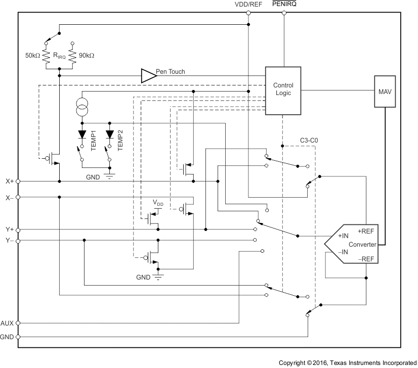 Figure 20. Analog Input Section (Simplified Diagram)
A unique configuration of low ON-resistance switches allows an unselected A-D converter input channel to provide power and an accompanying pin to provide ground for driving the touch panel. By maintaining a differential input to the converter and a differential reference input architecture, it is possible to negate errors caused by the driver switch ON-resistance.
7.3.3.1 Reference
The TSC2007-Q1 uses an external voltage reference that is applied to the VDD/REF pin. The upper reference voltage range is the same as the supply voltage range, which allows for simple, 1.2-V to 3.6-V, single-supply operation of the chip.
7.3.3.2 Reference Mode
There is a critical item regarding the reference when making measurements while the switch drivers are on. For this discussion, it is useful to consider the basic operation of the TSC2007-Q1 (see Figure 34). The application used in the following example shows the device being used to digitize a resistive touch screen. If the touch screen controller uses a single-ended reference mode, as shown in Figure 21, a measurement of the current Y position of the pointing device is made by connecting the X+ input to the A-D converter, turning on the Y+ and Y– drivers, and digitizing the voltage on X+. For this measurement, the resistance in the X+ lead does not affect the conversion; it does affect the settling time, but the resistance is usually small enough that this timing is not a concern. However, because the resistance between Y+ and Y– is fairly low, the ON-resistance of the Y drivers does make a small difference. Under the situation outlined so far, it would not be possible to achieve a 0-V input or a full-scale input regardless of where the pointing device is on the touch screen because some voltage is lost across the internal switches. In addition, the internal switch resistance is unlikely to track the resistance of the touch screen, providing an additional source of error. Therefore, the TSC2007-Q1 does not support single-ended reference mode.
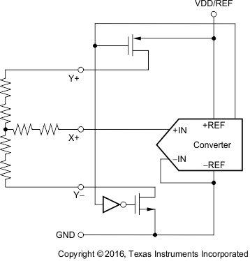 Figure 21. Simplified Diagram of Single-Ended Reference
This situation is resolved, as shown in Figure 22, by using the differential mode; the +REF and –REF inputs are connected directly to Y+ and Y–, respectively. This mode makes the A-D converter ratiometric. The result of the conversion is always a percentage of the external reference, regardless of how it changes in relation to the ON-resistance of the internal switches.
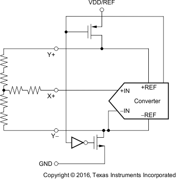 Figure 22. Simplified Diagram of Differential Reference
(Both Y Switches Enabled, X+ is Analog Input)
7.3.3.3 Touch Screen Settling
In some applications, external capacitors may be required across the touch screen to filter noise picked up by the touch screen (noise generated by the LCD panel or back-light circuitry). These capacitors provide a low-pass filter to reduce the noise, but they also cause a settling time requirement when the panel is touched. The settling time typically shows up as a gain error. The problem is that the input or reference has not settled to its final steady-state value before the A-D converter samples the inputs and provides the digital output. Additionally, the reference voltage may continue to change during the measurement cycle.
To resolve these settling-time problems, the TSC2007-Q1 can be commanded to turn on the drivers only without performing a conversion (see Table 4). Time can then be allowed, before the command is issued, to perform a conversion. Generally, the time it takes to communicate the conversion command over the I2C bus is adequate for the touch screen to settle.
7.3.3.4 Variable Resolution
The TSC2007-Q1 provides either 8-bit or 12-bit resolution for the A-D converter. Lower resolution is often practical for measuring slow changing signals such as touch pressure. Performing the conversions at lower resolution reduces the amount of time it takes for the A-D converter to complete its conversion process, which also lowers power consumption.
7.3.3.5 8-Bit Conversion
The TSC2007-Q1 provides an 8-bit conversion mode (M = 1) that can be used when faster throughput is required, and the digital result is not as critical (for example, measuring pressure). By switching to the 8-bit mode, a conversion result can be read by transferring only one data byte. The internal clock runs twice as fast at 4 MHz.
The faster clock shortens each conversion by four bits and reduces data transfer time, which results in fewer clock cycles and provides lower power consumption.
7.3.3.6 Conversion Clock and Conversion Time
The TSC2007-Q1 contains an internal clock, which drives the state machines inside the device that perform the many functions of the part. This clock is divided down to provide a clock that runs the A-D converter. The frequency of this clock is 4-MHz clock for 8-bit mode, and a 2-MHz clock for the 12-bit mode.
7.3.3.7 Data Format
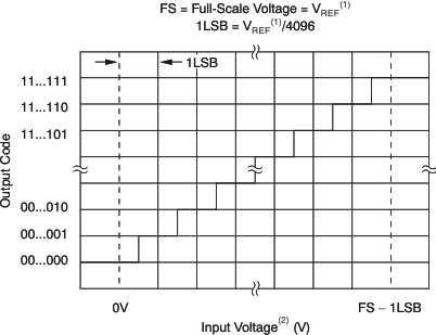
The TSC2007-Q1 output data are in straight binary format as shown in Figure 23. This figure shows the ideal output code for the given input voltage and does not include the effects of offset, gain, or noise.
7.3.3.8 Touch Detect
The PENIRQ pin can be used as an interrupt to the host. RIRQ is an internal pullup resistor with a programmable value of either 50 kΩ (default) or 90 kΩ. Write command 1011 (setup command) followed by data 0001 sets the pullup to 90 kΩ.
NOTE
The first three bits must be 0s and the select bit is the last bit. To change the pullup back to 50 kΩ, issue write command 1011 followed by data 0000.
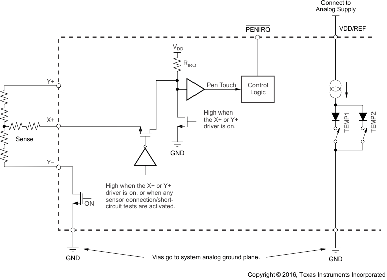
An example for the Y-position measurement is detailed in Figure 24. The PENIRQ output is pulled high by an internal pullup. While in power-down mode with PD0 = 0, the Y– driver is on and connected to GND, and the PENIRQ output is connected to the X+ input. When the panel is touched, the X+ input is pulled to ground through the touch screen, and the PENIRQ output goes low because of the current path through the panel to GND, initiating an interrupt to the processor. During the measurement cycle for X, Y, and Z position, the X+ input is disconnected from the PENIRQ pulldown transistor to eliminate any pullup resistor leakage current from flowing through the touch screen, thus causing no errors.
In addition to the measurement cycles for X, Y, and Z position, commands that activate the X-drivers, Y-drivers, and Y+ and X-drivers without performing a measurement also disconnect the X+ input from the PENIRQ pulldown transistor, and disable the pen-interrupt output function, regardless of the value of the PD0 bit. Under these conditions, the PENIRQ output is forced low. Furthermore, if the last command byte written to the TSC2007-Q1 contains PD0 = 1, the pen-interrupt output function is disabled and cannot detect when the panel is touched. To re-enable the pen-interrupt output function under these circumstances, a command byte must be written to the TSC2007-Q1 with PD0 = 0.
When the bus master sends the address byte with the R/W bit = 0, and the TSC2007-Q1 sends an acknowledge, the pen-interrupt function is disabled. If the command that follows the address byte contains PD0 = 0, then the pen-interrupt function is enabled at the end of a conversion. This action is approximately 100 µs (12-bit mode) or 50 µs (8-bit mode) after the TSC2007-Q1 receives a STOP or START condition, following the receipt of a command byte (see Figure 30 and Figure 29 for further details about when the conversion cycle begins).
In both cases previously listed, TI recommends that whenever the host writes to the TSC2007-Q1, the master processor masks the interrupt associated to PENIRQ. This masking prevents false triggering of interrupts when the PENIRQ line is disabled in the cases previously listed.
7.3.3.9 Preprocessing
The TSC2007-Q1 has a combined MAV filter (median value filter and averaging filter).
7.3.3.9.1 MAV Filter
If the acquired signal source is noisy because of the digital switching circuit, it may necessary to evaluate the data without noise. In this case, the median value filter operation helps remove the noise. The array of seven converted results is sorted first. The middle three values are then averaged to produce the output value of the MAV filter.
The MAV filter is applied to all measurements for all analog inputs including the touch screen inputs, temperature measurements TEMP1 and TEMP2, and auxiliary input AUX. To shorten the conversion time, the MAV filter may be bypassed through the setup command; see Table 4 and Table 5.
 Figure 25. MAV Filter Operation (Patent Pending)
7.4 Device Functional Modes
7.4.1 Power-On Reset (POR)
During TSC2007-Q1 power up, an internal power-on reset (POR) is automatically implemented. The POR brings the TSC to the default working condition, and checks the A0 and A1 pins for the two LSBs of the I2C address. The TSC2007-Q1 senses the power-up curve to decide whether or not to implement a POR.
It is required to follow the power-on and power-off slope and interval requirements, as provided in Electrical Characteristics, to ensure a proper POR of the TSC2007-Q1. Review Important Considerations to Assure a Safe POR to ensure a safe POR.
 Figure 26. Power-On Reset Timing
Table 1. Timing Requirements for Figure 26
| PARAMETER | TEST CONDITIONS | MIN | MAX | UNIT |
|---|---|---|---|---|
| VDD off ramp | TA = –40°C to 85°C | 2 | kV/s | |
| VDD off time | TA = –40°C to 85°C, VDD = 0 V | 1.2 | s | |
| TA = –20°C to 85°C, VDD = 0 V | 0.3 | s | ||
| VDD on ramp | TA = –40°C to 85°C | 12 | kV/s |
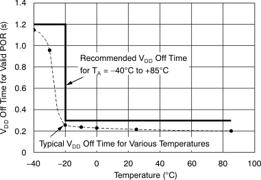 Figure 27. VDD Off Time vs Temperature
7.5 Programming
7.5.1 I2C Interface
The TSC2007-Q1 supports the I2C serial bus and data transmission protocol in all three defined modes: standard, fast, and high-speed. A device that sends data onto the bus is defined as a transmitter, and a device receiving data as a receiver. The device that controls the message is called a master. The devices that are controlled by the master are slaves. The bus must be controlled by a master device that generates the serial clock (SCL), controls the bus access, and generates the START and STOP conditions. The TSC2007-Q1 operates as a slave on the I2C bus. Connections to the bus are made through the open-drain I/O lines, SDA, and SCL.
The following bus protocol has been defined (see Figure 28):
- Data transfer may be initiated only when the bus is not busy.
- During data transfer, the data line must remain stable whenever the clock line is HIGH. Changes in the data line while the clock line is HIGH are interpreted as control signals.
Accordingly, the following bus conditions have been defined:
-
Bus Not Busy
Both data and clock lines remain HIGH.
-
Start Data Transfer
A change in the state of the data line, from HIGH to LOW, while the clock is HIGH, defines a START condition.
-
Stop Data Transfer
A change in the state of the data line, from LOW to HIGH, while the clock line is HIGH, defines the STOP condition.
-
Data Valid
The state of the data line represents valid data, when, after a START condition, the data line is stable for the duration of the HIGH period of the clock signal. There is one clock pulse per bit of data.
Each data transfer is initiated with a START condition and terminated with a STOP condition. The number of data bytes transferred between START and STOP conditions is not limited and is determined by the master device. The information is transferred byte-wise and each receiver acknowledges with a ninth-bit.
Within the I2C bus specifications, a standard mode (100-kHz clock rate), a fast mode (400-kHz clock rate), and a high-speed mode (1.7-MHz or 3.4-MHz clock rate) are each defined. The TSC2007-Q1 works in all three modes.
-
Acknowledge
Each receiving device, when addressed, is obliged to generate an acknowledge after the reception of each byte. The master device must generate an extra clock pulse that is associated with this acknowledge bit.
A device that acknowledges must pull down the SDA line during the acknowledge clock pulse in such a way that the SDA line is stable LOW during the HIGH period of the acknowledge clock pulse. Of course, setup and hold times must be taken into account. A master must signal an end of data to the slave by not generating an acknowledge bit on the last byte that has been clocked out of the slave. In this case, the slave must leave the data line HIGH to enable the master to generate the STOP condition.
Figure 28 details how data transfer is accomplished on the I2C bus. Depending upon the state of the R/W bit, two types of data transfer are possible:
- Data transfer from a master transmitter to a slave receiver. The first byte transmitted by the master is the slave address. Next follows a number of data bytes. The slave returns an acknowledge bit after the slave address and each received byte.
- Data transfer from a slave transmitter to a master receiver. The first byte, the slave address, is transmitted by the master. The slave then returns an acknowledge bit. Next, a number of data bytes are transmitted by the slave to the master. The master returns an acknowledge bit after all received bytes other than the last byte. At the end of the last received byte, a not-acknowledge is returned.
The master device generates all of the serial clock pulses and the START and STOP conditions. A transfer ends with a STOP condition or a repeated START condition. Because a repeated START condition is also the beginning of the next serial transfer, the bus is not released.
The TSC2007-Q1 may operate in the following two modes:
- Slave Receiver Mode: Serial data and clock are received through SDA and SCL. After each byte is received, an acknowledge bit is transmitted. START and STOP conditions are recognized as the beginning and end of a serial transfer. Address recognition is performed by hardware after reception of the slave address and direction bit.
- Slave Transmitter Mode: The first byte (the slave address) is received and handled as in the slave receiver mode. However, in this mode, the direction bit indicates that the transfer direction is reversed. Serial data are transmitted on SDA by the TSC2007-Q1 while the serial clock is input on SCL. START and STOP conditions are recognized as the beginning and end of a serial transfer.
7.5.1.1 I2C Fast or Standard Mode (F/S Mode)
In I2C Fast or Standard (F/S) mode, serial data transfer must meet the timing shown in the Specifications section.
In the serial transfer format of F/S mode, the master signals the beginning of a transmission to a slave with a START condition (S), which is a high-to-low transition on the SDA input while SCL is high. When the master has finished communicating with the slave, the master issues a STOP condition (P), which is a low-to-high transition on SDA while SCL is high, as shown in Figure 28. The bus is free for another transmission after a STOP condition has occurred. Figure 28 shows the complete F/S mode transfer on the I2C, 2-wire serial interface. The address byte, control byte, and data byte are transmitted between the START and STOP conditions. The SDA state is only allowed to change while SCL is low, except for the START and STOP conditions. Data are transmitted in 8-bit words. Nine clock cycles are required to transfer the data into or out of the device (8-bit word plus acknowledge bit).
 Figure 28. Complete Fast-Mode or Standard-Mode Transfer
7.5.1.2 I2C High-Speed Mode (HS Mode)
The TSC2007-Q1 can operate with high-speed I2C masters. To do so, the pullup resistor on SCL must be changed to an active pullup, as recommended in the I2C specification.
Serial data transfer format in High-Speed (HS) mode meets the Fast or Standard (F/S) mode I2C bus specification. HS mode can only commence after the following conditions (all of which are in F/S mode) exist:
- START condition (S)
- 8-bit master code (00001xxx)
- Not-acknowledge bit (N)
Figure 29 shows this sequence in more detail. HS-mode master codes are reserved 8-bit codes used only for triggering HS mode, and are not to be used for slave addressing or any other purpose. The master code indicates to other devices that an HS-mode transfer is about to begin and the connected devices must meet the HS-mode specification. Because no device is allowed to acknowledge the master code, the master code is followed by a not-acknowledge bit (N).
After the not-acknowledge bit (N) and SCL have been pulled up to a HIGH level, the master switches to HS mode and enables the current-source pullup circuit for SCL (at time tH shown in Figure 29). Because other devices can delay the serial transfer before tH by stretching the LOW period of SCL, the master enables the current-source pullup circuit when all devices have released SCL, and SCL has reached a HIGH level, thus speeding up the last part of the rise time of the SCL.
The master then sends a repeated START condition (Sr) followed by a 7-bit slave address with a R/W bit address, and receives an acknowledge bit (A) from the selected slave. After a repeated START (Sr) condition and after each acknowledge bit (A) or not-acknowledge bit (N), the master disables its current-source pullup circuit. This disabling enables other devices, such as the TSC2007-Q1, to delay the serial transfer (until the converted data are stored in the TSC internal shift register) by stretching the LOW period of SCL. The master re-enables its current-source pullup circuit again when all devices have released SCL, and SCL reaches a HIGH level, which speeds up the last part of the SCL signal rise time.
Data transfer continues in HS mode after the next repeated START (Sr), and only switches back to F/S mode after a STOP condition (P). To reduce the overhead of the master code, it is possible for the master to link a number of HS-mode transfers, separated by repeated START conditions (Sr).
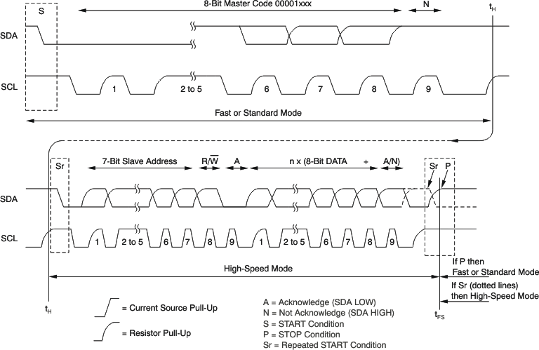 Figure 29. Complete High-Speed Mode Transfer
7.5.2 Digital Interface
7.5.2.1 Address Byte
The TSC2007-Q1 has a 7-bit slave address word. The first five bits (MSBs) of the slave address are factory-preset to comply with the I2C standard for A-D converters and are always set at 10010. The logic state of the address input pins (A1–A0) determines the two LSBs of the device address to activate communication. Therefore, a maximum of four devices with the same preset code can be connected on the same bus at one time.
The A1–A0 address inputs are read whenever an address byte is received, and must be connected to the supply pin (VDD/REF) or the ground pin (GND). The slave address is latched into the TSC2007-Q1 on the falling edge of SCL after the R/W bit has been received by the slave.
The last bit of the address byte (R/W) defines the operation to be performed. When set to a 1, a read operation is selected; when set to a zero, a write operation is selected. Following the START condition, the TSC2007-Q1 monitors the SDA bus, checking the device type identifier being transmitted. Upon receiving the 10010 code, the appropriate device select bits, and the R/W bit, the slave device outputs an acknowledge signal on the SDA line.
Table 2. I2C Slave Address Byte
| MSB D7 |
D6 | D5 | D4 | D3 | D2 | D1 | LSB D0 |
|---|---|---|---|---|---|---|---|
| 1 | 0 | 0 | 1 | 0 | A1 | A0 | R/W |
Bit D0: R/W
1: I2C master read from TSC (I2C read addressing).
0: I2C master write to TSC (I2C write addressing).
7.5.2.2 Command Byte
Table 3. Command Byte Definition (Excluding the Setup Command)(1)
| BIT | NAME | DESCRIPTION |
|---|---|---|
| D7–D4 | C3–C0 | Converter function select bits: These bits select the input to be converted and the converter function to be executed, activate the drivers, and configure the PENIRQ pullup resistor (RIRQ). Table 4 lists the possible converter functions. All Converter Function Select bits as detailed in Table 4, except for the setup command (1011). |
| D3–D2 | PD1–PD0 | Power-down bits: These two bits select the power-down mode that the TSC2007-Q1 enters after the current command completes, as shown in Table 3. It is recommended to set PD0 = 0 in each command byte to get the lowest power consumption possible. If multiple X, Y, and Z position measurements are done one right after another (such as when averaging), PD0 = 1 leaves the touch screen drivers on at the end of each conversion cycle. 00: Power down between cycles. PENIRQ enabled. 01: A-D converter on. PENIRQ disabled. 10: A-D converter off. PENIRQ enabled. 11: A-D converter on. PENIRQ disabled. |
| D1 | M | Mode bit 0: 12-bit (Lower speed referred to as the 2-MHz clock). 1: 8-bit (Higher speed referred to as the 4-MHz clock). |
| D0 | X | Do not care. |
When the TSC2007-Q1 powers up, the power-down bits must be written to ensure that the device is placed into the mode that achieves the lowest power. Therefore, immediately after power up, send a command byte that sets PD1 = PD0 = 0, so that the device is in the lowest power mode, powering down between conversions.
Table 4. Converter Function Select
| C3 | C2 | C1 | C0 | FUNCTION | INPUT TO A-D CONVERTER | X-DRIVERS | Y-DRIVERS | ACK | REFERENCE MODE |
|---|---|---|---|---|---|---|---|---|---|
| 0 | 0 | 0 | 0 | Measure TEMP0 | TEMP0 | OFF | OFF | Y | Single-Ended |
| 0 | 0 | 0 | 1 | Reserved | — | OFF | OFF | N | Single-Ended |
| 0 | 0 | 1 | 0 | Measure AUX | AUX | OFF | OFF | Y | Single-Ended |
| 0 | 0 | 1 | 1 | Reserved | — | OFF | OFF | N | Single-Ended |
| 0 | 1 | 0 | 0 | Measure TEMP1 | TEMP1 | OFF | OFF | Y | Single-Ended |
| 0 | 1 | 0 | 1 | Reserved | — | OFF | OFF | N | Single-Ended |
| 0 | 1 | 1 | 0 | Reserved | — | OFF | OFF | N | Single-Ended |
| 0 | 1 | 1 | 1 | Reserved | — | OFF | OFF | N | Single-Ended |
| 1 | 0 | 0 | 0 | Activate X-drivers | — | ON | OFF | Y | Differential |
| 1 | 0 | 0 | 1 | Activate Y-drivers | — | OFF | ON | Y | Differential |
| 1 | 0 | 1 | 0 | Activate Y+, X-drivers | — | X– ON | Y+ ON | Y | Differential |
| 1 | 0 | 1 | 1 | Setup command(1) | — | OFF | OFF | N | — |
| 1 | 1 | 0 | 0 | Measure X position | Y+ | ON | OFF | Y | Differential |
| 1 | 1 | 0 | 1 | Measure Y position | X+ | OFF | ON | Y | Differential |
| 1 | 1 | 1 | 0 | Measure Z1 position | X+ | X– ON | Y+ ON | Y | Differential |
| 1 | 1 | 1 | 1 | Measure Z2 position | Y– | X– ON | Y+ ON | Y | Differential |
Table 5. Command Byte Definition for the Setup Command
| BIT | NAME | DESCRIPTION |
|---|---|---|
| D7–D4 | C3–C0 | Setup command; must write 1011. |
| D3–D2 | PD1–PD0 | Reserved; must write 00. |
| D1 | Filter control | 0: Use the onboard MAV filter (default). 1: Bypass the onboard MAV filter. |
| D0 | RIRQ select | PENIRQ pullup resistor (RIRQ) select 0: RIRQ = 50 kΩ (default). 1: RIRQ = 90 kΩ. |
7.5.2.3 Start a Converter Function or Write Cycle
A conversion or write cycle begins when the master issues the address byte containing the slave address of the TSC2007-Q1, with the eighth bit equal to a 0 (R/W = 0), as shown in Table 2. Once the eighth bit has been received, and the address matches the A1–A0 address input pin setting, the TSC2007-Q1 issues an acknowledge.
When the master receives the acknowledge bit from the TSC2007-Q1, the master writes the command byte to the slave (see Table 3). After the command byte is received by the slave, the slave issues another acknowledge bit. The master then ends the write cycle by issuing a repeated START or a STOP condition, as shown in Figure 30.
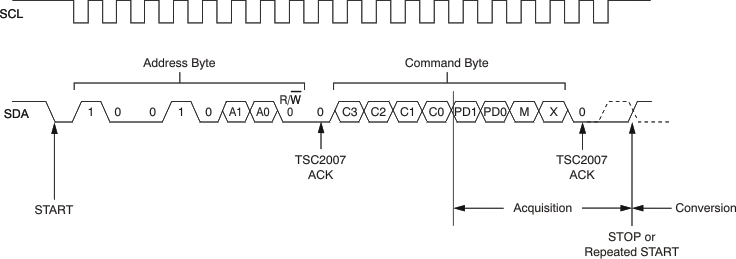 Figure 30. Complete I2C Serial Write Transmission
If the master sends additional command bytes after the initial byte, but before sending a STOP or repeated START condition, the TSC2007-Q1 does not acknowledge those bytes.
The input multiplexer channel for the A-D converter is selected when bits C3 through C0 are clocked in. If the selected channel is an X, Y, or Z position measurement, the appropriate drivers turn on once the acquisition period begins.
When R/W = 0, the input sample acquisition period starts on the falling edge of SCL when the C0 bit of the command byte has been latched, and ends when a STOP or repeated START condition has been issued. A-D conversion starts immediately after the acquisition period. The multiplexer inputs to the A-D converter are disabled once the conversion period starts. However, if an X, Y, or Z position is being measured, the respective touch screen drivers remain on during the conversion period. A complete write cycle is shown in Figure 30.
7.5.2.4 Read a Conversion or Read Cycle
For best performance, the I2C bus must remain in an idle state while an A-D conversion is taking place. This idling prevents digital clock noise from affecting the bit decisions being made by the TSC2007-Q1. The master must wait for at least 10 µs before attempting to read data from the TSC2007-Q1 to realize this best performance. However, the master does not need to wait for a completed conversion before beginning a read from the slave, if full 12-bit performance is not necessary.
Data access begins with the master issuing a START condition followed by the address byte (see Table 2) with R/W = 1.
When the eighth bit has been received and the address matches, the slave issues an acknowledge. The first byte of serial data then follows (D11–D4, MSB first).
After the first byte has been sent by the slave, it releases the SDA line for the master to issue an acknowledge. The slave responds with the second byte of serial data upon receiving the acknowledge from the master (D3–D0, followed by four 0 bits). The second byte is followed by a NOT acknowledge bit (ACK = 1) from the master to indicate that the last data byte has been received. If the master somehow acknowledges the second data byte, invalid data are returned (FFh). This condition applies to both 12-bit and 8-bit modes. See Figure 31 for a complete I2C read transmission.
 Figure 31. Complete I2C Serial Read Transmission
7.5.2.5 Throughput Rate and I2C Bus Traffic
Although the internal A-D converter has a sample rate of up to 200 kSPS, the throughput presented at the bus is much lower. The rate is reduced because preprocessing manages the redundant work of filtering out noise. The throughput is further limited by the I2C bus bandwidth. The effective throughput is approximately 20 kSPS at 8-bit resolution, or 10 kSPS at 12-bit resolution. This preprocessing saves a large portion of the I2C bandwidth for the system to use on other devices.
Each sample and conversion takes 19 CCLK cycles (12-bit), or 16 CCLK cycles (8-bit). For a typical internal 4-MHz OSC clock, the frequency actually ranges from 3.66 MHz to 3.82 MHz. For VDD = 1.2 V, the frequency reduces to 3.19 MHz, which gives a 3.19 MHz / 16 = 199 kSPS raw A-D converter sample rate.
7.5.2.5.1 12-Bit Operation
For 12-bit operation, sending the conversion result across the I2C bus takes 49 bus clocks (SCL clock). Each write cycle takes 20 I2C cycles (START, STOP, address byte, 2 ACKs, and command byte). Each read cycle takes 29 I2C cycles (START, STOP, address byte, 3 ACKs, and data bytes 1 and 2). Seven sample-and-convert operations take 19 × 7 internal clocks to complete. The MAV filter loop requires 19 internal clocks. For VDD = 1.2 V, the complete processed data cycle time calculations are shown in Table 6. Because the first acquisition cycle overlaps with the I/O cycle, four CCLKs must be deducted from the total CCLK cycles. For 12-bit mode, (19 × 7 + 19) – 4 = 148 CCLKs plus I/O are required.
7.5.2.5.2 8-Bit Operation
For 8-bit operation, sending the conversion result across the I2C bus takes 40 bus clocks (SCL clock). Each write cycle takes 20 I2C cycles (START, STOP, address byte, 2 ACKs, and command byte). Each read cycle takes 20 I2C cycles (START, STOP, address byte, 2 ACKs, and data byte 1). Seven sample-and-convert operations takes 16×7 internal clocks to complete. The MAV filter loop requires 19 internal clocks. For VDD = 1.2 V, the complete processed data cycle time calculations are shown in Table 6. Because the first acquisition cycle overlaps with the I/O cycle, four CCLKs must be deducted from the total CCLK cycles. For 8-bit mode, (16 × 7 + 19) – 4 = 127 CCLKs plus I/O are required.
Table 6. Measurement Cycle Time Calculations
| STANDARD MODE: 100 kHz (Period = 10 µs) | |
|---|---|
| 8-Bit | 40 × 10 µs + 127 × 313 ns = 439.8 µs (2.27 kSPS through the I2C bus) |
| 12-Bit | 49 × 10 µs + 148 × 625 ns = 582.5 µs (1.72 kSPS through the I2C bus) |
| FAST MODE: 400 kHz (Period = 2.5 µs) | |
| 8-Bit | 40 × 2.5 µs + 127 × 313 ns = 139.8 µs (7.15 kSPS through the I2C bus) |
| 12-Bit | 49 × 2.5 µs + 148 × 625 ns = 215 µs (4.65 kSPS through the I2C bus) |
| HIGH-SPEED MODE: 1.7 MHz (Period = 588 ns) | |
| 8-Bit | 40 × 588 ns + 127 × 313 ns = 63.3 µs (15.79 kSPS through the I2C bus) |
| 12-Bit | 49 × 588 ns + 148 × 625 ns = 121.3 µs (8.24 kSPS through the I2C bus) |
| HIGH-SPEED MODE: 3.4 MHz (Period = 294 ns) | |
| 8-Bit | 40 × 294 ns + 127 × 313 ns = 51.6 µs (19.39 kSPS through the I2C bus) |
| 12-Bit | 49 × 294 ns + 148 × 625 ns = 106.9 µs (9.35 kSPS through the I2C bus) |
As an example, use VDD = 1.2 V and 12-bit mode with the Fast-mode I2C clock (fSCL = 400 kHz). The equivalent TSC throughput is at least seven times faster than the effective throughput across the bus (4.65 k × 7 = 32.55 kSPS). The supply current to the TSC for this rate and configuration is 128 µA. To achieve an equivalent sample throughput of 8.2 kSPS using the device without preprocessing, the TSC2007-Q1 consumes only (8.2 or 32.55) × 128 µA = 32.24 µA.
Table 7. Effective and Equivalent Throughput Rates
| SUPPLY VOLTAGE | I2C BUS SPEED (fSCL) | RESOLUTION | TSC CONVERSION CYCLE TIME (µs) | EFFECTIVE THROUGHPUT (kSPS) | EQUIVALENT THROUGHPUT (kSPS) | SCL CYCLES | CCLK CYCLES | fCCLK (kHz) | CCLK PERIODS (ns) |
|---|---|---|---|---|---|---|---|---|---|
| 2.7 V | 100 kHz Standard |
8-bit | 433.6 | 2.31 | 16.14 | 40 | 127 | 3780 | 264.6 |
| 12-bit | 568.7 | 1.76 | 12.31 | 49 | 148 | 1880 | 531.9 | ||
| 400 kHz Fast |
8-bit | 133.6 | 7.49 | 52.4 | 40 | 127 | 3780 | 264.6 | |
| 12-bit | 201.2 | 4.97 | 34.79 | 49 | 148 | 1880 | 531.9 | ||
| 1.7 MHz High-Speed |
8-bit | 57.1 | 17.5 | 122.53 | 40 | 127 | 3780 | 264.6 | |
| 12-bit | 107.5 | 9.3 | 65.09 | 49 | 148 | 1880 | 531.9 | ||
| 3.4 MHz High-Speed |
8-bit | 45.4 | 22.04 | 154.31 | 40 | 127 | 3780 | 264.6 | |
| 12-bit | 93.1 | 10.74 | 75.16 | 49 | 148 | 1880 | 531.9 | ||
| 1.8 V | 100 kHz Standard |
8-bit | 434.7 | 2.3 | 16.1 | 40 | 127 | 3660 | 273.2 |
| 12-bit | 570.9 | 1.75 | 12.26 | 49 | 148 | 1830 | 546.4 | ||
| 400 kHz Fast |
8-bit | 134.7 | 7.42 | 51.97 | 40 | 127 | 3660 | 273.2 | |
| 12-bit | 203.4 | 4.92 | 34.42 | 49 | 148 | 1830 | 546.4 | ||
| 1.7 MHz High-Speed |
8-bit | 58.2 | 17.17 | 120.22 | 40 | 127 | 3660 | 273.2 | |
| 12-bit | 109.7 | 9.12 | 63.81 | 49 | 148 | 1830 | 546.4 | ||
| 3.4 MHz High-Speed |
8-bit | 46.5 | 21.52 | 150.65 | 40 | 127 | 3660 | 273.2 | |
| 12-bit | 95.3 | 10.49 | 73.46 | 49 | 148 | 1830 | 546.4 | ||
| 1.2 V | 100 kHz Standard |
8-bit | 439.8 | 2.27 | 15.92 | 40 | 127 | 3190 | 313.5 |
| 12-bit | 582.5 | 1.72 | 12.02 | 49 | 148 | 1600 | 625 | ||
| 400 kHz Fast |
8-bit | 139.8 | 7.15 | 50.07 | 40 | 127 | 3190 | 313.5 | |
| 12-bit | 215 | 4.65 | 32.56 | 49 | 148 | 1600 | 625 | ||
| 1.7 MHz High-Speed |
8-bit | 63.3 | 15.79 | 110.51 | 40 | 127 | 3190 | 313.5 | |
| 12-bit | 121.3 | 8.24 | 57.7 | 49 | 148 | 1600 | 625 | ||
| 3.4 MHz High-Speed |
8-bit | 51.6 | 19.39 | 135.72 | 40 | 127 | 3190 | 313.5 | |
| 12-bit | 106.9 | 9.35 | 65.47 | 49 | 148 | 1600 | 625 |
 Figure 32. Data Acquisition Cycle (Filter Enabled)
 Figure 33. Data Acquisition Cycle (Filter Disabled)
