SCDS335A September 2012 – August 2014 TSU8111
PRODUCTION DATA.
- 1 Features
- 2 Applications
- 3 Description
- 4 Revision History
- 5 Pin Configuration and Functions
- 6 Specifications
-
7 Detailed Description
- 7.1 Overview
- 7.2 Functional Block Diagram
- 7.3 Feature Description
- 7.4 Device Functional Modes
- 7.5 Programming
- 7.6
Register Map
- 7.6.1 Device ID (01h) Register Field Descriptions
- 7.6.2 Control (02h) Register Field Descriptions
- 7.6.3 Interrupt 1 (03h) Register Field Descriptions
- 7.6.4 Interrupt 2 (04h) Register Field Descriptions
- 7.6.5 Interrupt Mask 1 (05h) Register Field Descriptions
- 7.6.6 Interrupt Mask 2 (06h) Register Field Descriptions
- 7.6.7 ADC (07h) Register Field Descriptions
- 7.6.8 Timing Set 1 (08h) Register Field Descriptions
- 7.6.9 Timing Set 2 (09h) Register Field Descriptions
- 7.6.10 Device Type 1 (0Ah) Register Field Descriptions
- 7.6.11 Device Type 2 (0Bh) Register Field Descriptions
- 7.6.12 Button 1 (0Ch) Register Field Descriptions
- 7.6.13 Button 2 (0Dh) Register Field Descriptions
- 7.6.14 Manual SW 1 (13h) Register Field Descriptions
- 7.6.15 Manual SW 2 (14h) Register Field Descriptions
- 7.6.16 Reset (1Bh) Register Field Descriptions
- 7.6.17 Charger control 1 (20h) Register Field Descriptions
- 7.6.18 Charger control 2 (21h) Register Field Descriptions
- 7.6.19 Battery Charger Control 3 (22h) Register Field Descriptions
- 7.6.20 Charger Interrupt (24h) Register Field Descriptions
- 7.6.21 Charger Interrupt Mask (25h) Register Field Descriptions
- 7.6.22 Charger Status (26h) Register Field Descriptions
- 8 Application and Implementation
- 9 Power Supply Recommendations
- 10Layout
- 11Device and Documentation Support
- 12Mechanical, Packaging, and Orderable Information
Package Options
Mechanical Data (Package|Pins)
- YFP|20
Thermal pad, mechanical data (Package|Pins)
Orderable Information
7 Detailed Description
7.1 Overview
The TSU8111 is designed to interface a portable device (PD) to external peripherals through a micro-USB connector.
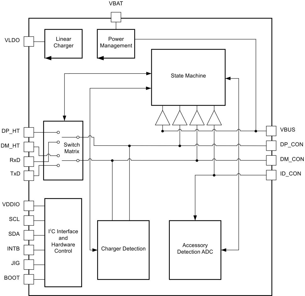
The device will automatically detect accessories via the mini-USB or micro-USB 5-pin connectors. The type of accessory detected will be stored in the TSU8111’s I2C registers, and can be read by the host processor. The TSU8111 has a network of USB 2.0 High Speed switches that can be automatically opened and closed based on the accessory detected. See Automatic Switching Mode for details of which switches are closed during each mode of operation. The TSU8111 also offers a manual switching mode through I2C, allowing the host processor to decide which switches will be opened and closed.The TSU8111 also provides a linear charger with a maximum programmable charging current of 950 mA.
7.2 Functional Block Diagram
7.3 Feature Description
7.3.1 Linear Charger
The TSU8111 has a linear battery charger with charging currents adjustable from 200 mA to 950 mA. If 3.7 V < VBUS < 7.5 V and VBUS > VBAT + 250 mV, then the charger starts charging automatically. If VBAT < VPRECHG, the device starts with a pre-charge mode with a charging current of 90 mA. Once VBAT reaches VPRECHG, the device switches to fast charge mode with soft start. When VBAT approaches VSET, constant-voltage (CV) charging mode starts with programmed regulation voltage. At CV mode, if the charging current reaches the programmed full charge current, the TSU8111 will generate an interrupt to the host indicating a full charge and will start the charger shutoff timer. If the shutoff timer is disabled, the charger stays at CV mode until stopped by the host processor.
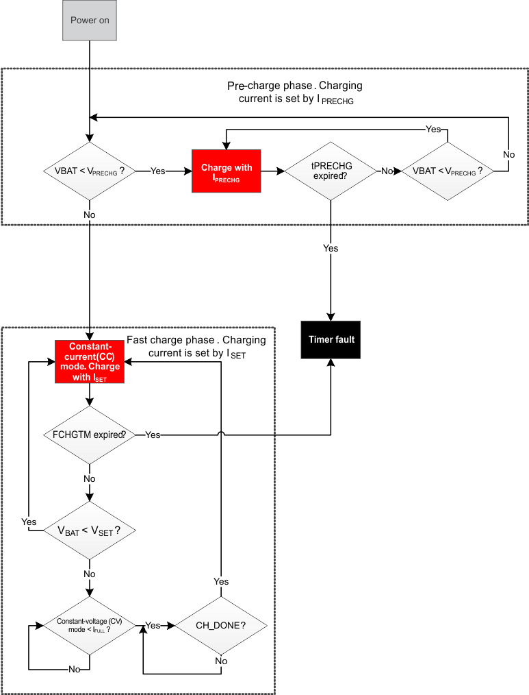 Figure 2. TSU8111 Charger Flow Chart
7.3.2 Voltage Protection
7.3.2.1 Overvoltage Protection
When VBUS rises above VBUS(OVP), the linear charger is turned off, removing power from the circuit. The OVP EN interrupt bit is set high when an overvoltage condition is detected. When the input voltage returns below VBUS(OVP) – VBUS(OVP(hys)) and remains above VBUS(UVLO) , the charger is turned on again.
7.3.2.2 Undervoltage Protection
The TSU8111 is powered off when VBUS and VBAT are below the lower thresholds of VBUS(UVLO) and VBAT(UVLO). When VBAT rises above 2.5 V, the device will be turned on but the linear charger will remain powered off. Both the TSU8111 and the linear charger will only be turned on when VBUS > 3.7 V and VBUS – VBAT > 250 mV.
7.3.3 Power-on Reset
When power is applied to VBAT, an internal power-on reset holds the TSU8111 in a reset condition. When VBAT reaches VPOR, the TSU8111 I2C registers and state machine initialize to their default states.
After the initial power-up phase, VBAT must be lowered below 0.2 V and then back up to VDDIO to initiate a power reset cycle.
7.3.4 Software Reset
To initiate a software reset on the TSU8111, perform the steps below:
- Hold SDA and SCL low for at least 30 ms to reset the digital logic of the TSU8111.
- Write a 1 to bit 0 of register 1Bh. This will reset the TSU8111, and the bit will be cleared after the reset. After the reset, INTB will keep low until the INT Mask bit of register 02h is cleared.
7.3.5 Power Supervisor
The TSU8111 uses VBAT as the primary supply voltage. VBUS is the secondary supply. VDDIO is used for I2C communication.
7.4 Device Functional Modes
7.4.1 Standby Mode
Standby mode is the default mode upon power up and occurs when no accessory is attached. During this time, the VBUS and ID lines are continually monitored through comparators to determine when an accessory is attached. If an accessory is attached, then the TSU8111 will enter either automatic or manual switching mode, depending on bit 2 in register 02h.
7.4.2 Automatic Switching Mode
The TSU8111 uses a current source and an internal comparator to detect a resistance on the ID pin. The current source creates VID on the ID pin, which is compared to a changing VREF input to the comparator. An incrementing 5-bit counter increases VREF until the comparator output changes. At this point, the TSU8111 latches the 5-bit counter value and determines the accessory type from Table 1.
When the TSU8111 detects VBUS but no ID resistor, the TSU8111 runs charger detection on the DP and DM lines. The TSU8111 can detect chargers compatible with the USB Battery Charging Specification version 1.1 (BCv1.1). The switch status for the BCv1.1 charger types can be found at the end of Table 1.
Table 1. Accessory and Charger Detection Lookup Table
| ACCESSORY | DETECTED IMPEDANCE ON ID (kΩ) | RESISTOR TOLERANCE (%) | 5-BIT COUNTER ADC VALUE | SWITCH STATE | FACTORY CABLE | ||
|---|---|---|---|---|---|---|---|
| DP / DM | |||||||
| DP_HT / DM_HT | RxD / TxD | JIG | BOOT | ||||
| OTG | 0 | N/A | 00000 | ON | OFF | OFF | OFF |
| MHL | 1 | 5 | 00000 | OFF | OFF | OFF | OFF |
| Audio Device Type 3 | 28.7 | 5 | 01110 | OFF | OFF | OFF | OFF |
| Reserved Accessory #1 | 34 | 5 | 01111 | OFF | OFF | OFF | OFF |
| Reserved Accessory #2 | 40.2 | 5 | 10000 | OFF | OFF | OFF | OFF |
| Reserved Accessory #3 | 49.9 | 5 | 10001 | OFF | OFF | OFF | OFF |
| Reserved Accessory #4 | 64.9 | 5 | 10010 | OFF | OFF | OFF | OFF |
| Audio Device Type 2 | 80.27 | 5 | 10011 | OFF | OFF | OFF | OFF |
| Phone Powered Device | 102 | 5 | 10100 | OFF | ON | OFF | OFF |
| TTY Converter | 121 | 5 | 10101 | OFF | OFF | OFF | OFF |
| UART Cable | 150 | 5 | 10110 | OFF | ON | OFF | OFF |
| Type 1 Charger | 200 | 5 | 10111 | ON | OFF | OFF | OFF |
| Factory Mode Cable – Boot Off USB | 255 | 5 | 11000 | ON | OFF | ON | OFF |
| Factory Mode Cable – Boot On USB | 301 | 5 | 11001 | ON | OFF | ON | ON |
| Audio / Video Cable | 365 | 5 | 11010 | OFF | OFF | OFF | OFF |
| Type 2 Charger | 442 | 5 | 11011 | ON | OFF | OFF | OFF |
| Factory Mode Cable – Boot Off UART | 523 | 5 | 11100 | OFF | ON | ON | OFF |
| Factory Mode Cable – Boot On UART | 619 | 5 | 11101 | OFF | ON | ON | ON |
| Stereo Headset with Remote (Audio Device Type 1) | 1000.07 | 10 | 11110 | OFF | OFF | OFF | OFF |
| Monio/Stereo Headset (Audio Device Type 1) | 1002 | 10 | 11110 | OFF | OFF | OFF | OFF |
| No ID | N/A | N/A | 11111 | OFF | OFF | OFF | OFF |
| USB Standard Downstream Port (SDP) | N/A | N/A | 11111 | ON | OFF | OFF | OFF |
| USB Charging Downstream Port (CDP) | N/A | N/A | 11111 | ON | OFF | OFF | OFF |
| Dedicated Charging Port (DCP) | N/A | N/A | 11111 | OFF | OFF | OFF | OFF |
7.4.3 Manual Switching Mode
Write a 0 to bit 2 of register 02h to enable manual switching mode. The switch status of DP and DM can then be controlled by writing to register 13h [7:2]. See Register Map for details about switch status using register 13h.
7.5 Programming
The bidirectional I2C bus consists of the serial clock (SCL) and serial data (SDA) lines. Both lines must be connected to a positive supply via a pullup resistor when connected to the output stages of a device. Data transfer may be initiated only when the bus is not busy.
I2C communication with this device is initiated by the master sending a START condition, a high-to-low transition on the SDA input/output while the SCL input is high (see Figure 3). After the start condition, the device address byte is sent, most significant bit (MSB) first, including the data direction bit (R/W). This device does not respond to the general call address. After receiving the valid address byte, this device responds with an ACK, a low on the SDA input/output during the high of the ACK-related clock pulse.
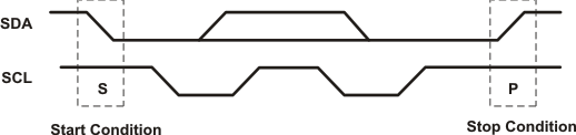 Figure 3. Definition of START and Stop Conditions
The data byte follows the address ACK. The R/W bit is kept low for transfer from the master to the slave. The data byte is followed by an ACK sent from this device. Data are the output only if complete bytes are received and acknowledged. The output data is valid at time tpv after the low-to-high transition of SCL, during the clock cycle for the ACK.
On the I2C bus, only one data bit is transferred during each clock pulse. The data on the SDA line must remain stable during the high pulse of the clock period, as changes in the data line at this time are interpreted as control commands (START or STOP). See Figure 4.
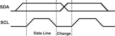 Figure 4. Bit Transfer
A STOP condition, a low-to-high transition on the SDA input/output while the SCL input is high, is sent by the master (see Figure 3).
The number of data bytes transferred between the START and STOP conditions from transmitter to receiver is not limited. Each byte of eight bits is followed by one ACK bit. The transmitted must release the SDA line before the receiver can send an ACK bit.
A slave receiver that is addressed must generate an ACK after the reception of each byte. The device that acknowledges has to pull down the SDA line during the ACK clock pulse so that the SDA line is stable low during the high pulse of the ACK-related clock period (see Figure 5). Setup and hold times must be taken into account.
 Figure 5. Acknowledgement on I2C Bus
7.5.1 Writes
Data is transmitted to the TSU8111 by sending the device slave address and setting the LSB to a logic 0 (see Figure 6 for device address). The command byte is sent after the address and determines which register receives the data that follows the command byte. The next byte is written to the specified register on the rising edge of the ACK clock pulse.
 Figure 6. Repeated Data Write to a Single Register
 Figure 7. Burst Data Write to Multiple Registers
7.5.2 Reads
The bus master must first send the TSU8111 slave address with the LSB set to logic 0. The command byte is sent after the address and determines which register is accessed. After a restart, the device slave address is sent again but, this time, the LSB is set to logic 1. Data from the register defined by the command byte then is sent by the TSU8111. Data is clocked into the SDA output shift register on the rising edge of the ACK clock pulse, see Figure 8.
 Figure 8. Repeated Data Read from a Single Register – Combined Mode
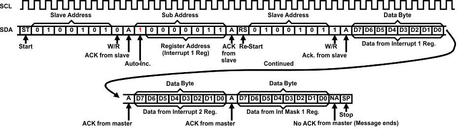 Figure 9. Burst Data Read from Multiple Registers – Combined Mode
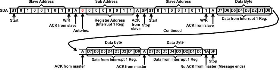 Figure 10. Repeated Data Read from a Single Register – Split Mode
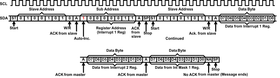 Figure 11. Burst Data Read from Multiple Registers – Split Mode
Additional notes on I2C interface:
- SDA is pulled low on ACK from either the slave or the master.
- Register writes always require sub-address writes before the first data byte.
- Repeated data writes to a single register continue indefinitely until stop or restart.
- Repeated data reads from a single register continue indefinitely until no ACK from master.
- Burst data writes start at the specified register address, then advance to the next register address, even to the read-only registers. For these registers, data write appears to occur, though no data are changed by the writes. After register 14h is written, writing resumes to register 01h and continues until stop or restart.
- Burst data reads start at the specified register address, then advance to the next register address. Once register 14h is read, reading resumes from register 01h and continues until no ACK from master.
7.6 Register Map(1)(2)
| ADDR | REGISTER | TYPE | RESET VALUE | BIT 7 | BIT 6 | BIT 5 | BIT 4 | BIT 3 | BIT 2 | BIT 1 | BIT 0 |
|---|---|---|---|---|---|---|---|---|---|---|---|
| 01h | Device ID | R | 1011010 | Version ID | Vendor ID | ||||||
| 02h | Control | R/W | xxx11111 | Switch Open | Raw Data | Manual Sw. | Wait | INT Mask | |||
| 03h | Interrupt 1 | R | x0000000 | VBUS | OVP EN | LKR | LKP | KP | Detach | Attach | |
| 04h | Interrupt 2 | R | x0000000 | OTP EN | CONNECT | Stuck Key RCV | Stuck Key | ADC Change |
Reserved Attach |
A/V Charging | |
| 05h | Interrupt Mask 1 | R/W | x0000000 | VBUS | OVP EN | LKR | LKP | KP | Detach | Attach | |
| 06h | Interrupt Mask 2 | R/W | x0000000 | OTP EN | CONNECT | Stuck Key RCV | Stuck Key | ADC Change |
Reserved Attach |
Charging A/V | |
| 07h | ADC | R | xxx11111 | ADC Value | |||||||
| 08h | Timing Set 1 | R/W | 0 | Key Press | Device Wake Up | ||||||
| 09h | Timing Set 2 | R/W | 0 | Switching Wait | Long Key Press | ||||||
| 0Ah | Device Type 1 | R | 0 | USB OTG | DCP | CDP | Type 1 / Type 2 charger | UART | USB | VBUS | MHL |
| 0Bh | Device Type 2 | R | 0 | Audio Type 3 |
Audio / Video | TTY | PPD | JIG UART OFF | JIG UART ON | JIG USB OFF |
JIG USB ON |
| 0Ch | Button 1 | R | 0 | 7 | 6 | 5 | 4 | 3 | 2 | 1 | Send End |
| 0Dh | Button 2 | R | x0000000 | Unknown | Error | 12 | 11 | 10 | 9 | 8 | |
| 13h | Manual SW 1 | R/W | 000000xx | DM Switching | DP Switching | ||||||
| 14h | Manual SW 2 | R/W | xxxx00xx | BOOT SW | JIG ON | ||||||
| 1Bh | Reset | W | 11111111 | Reset | |||||||
| 20h | Charger Control 1 | R/W | 11000 | CH DIS | CHRSTTH | CHENOV | FCMEN | FCHGTM | |||
| 21h | Charger Control 2 | R/W | 11010 | IFULL | CV SET | ||||||
| 22h | Charger Control 3 | R//W | 11010101 | OVPV | AUTOSTOP | ISET L | ISET | ||||
| 24h | Charger Interrupt | R | xx0xxxxx | CH FAULT | CH DONE | CH CV | CH FC | CH PC | CH IDLE | ||
| 25h | Charger Interrupt Mask | R/W | xx0xxxxx | CH FAULT | CH DONE | CH CV | CH FC | CH PC | CH IDLE | ||
| 26h | Charger Status | R | xx0xxxxx | FTE | PTE | CH FAULT | CH DONE | CH CV | CH FC | CH PC | CH IDLE |
7.6.1 Device ID (01h) Register Field Descriptions
Table 2. Device ID (01h) Register Field Descriptions
| Bit | Field | Type | Reset | Description |
|---|---|---|---|---|
| 7-3 | Version ID | R | 01011 | Unique identifier for chip version (01011) |
| 2-0 | Vendor ID | R | 010 | Unique identifier 010 for Texas Instruments |
7.6.2 Control (02h) Register Field Descriptions
Table 3. Control (02h) Register Field Descriptions
| Bit | Field | Type | Reset | Description |
|---|---|---|---|---|
| 7-5 | Blank | N/A | N/A | N/A |
| 4 | Switch Open | R/W | 1 | 0: Open all switches 1: Automatic switching by accessory detection |
| 3 | Raw Data | R/W | 1 | 0: Continue reading ID pin resistance after impedance has been detected 1: When ID resistance is connected, do not run ID detection again until the next attach/detach |
| 2 | Manual Sw. | R/W | 1 | 0: Manual switching mode enabled and controlled by register 13h 1: Automatic switching by accessory detection |
| 1 | Wait | R/W | 1 | 0: Wait until host resets this bit high 1: Wait until switching timer has expired |
| 0 | INT Mask | R/W | 1 | 0: Unmask interrupt 1: Mask interrupt |
7.6.3 Interrupt 1 (03h) Register Field Descriptions
Table 4. Interrupt 1 (03h) Register Field Descriptions
| Bit | Field | Type | Reset | Description |
|---|---|---|---|---|
| 7 | Unused | N/A | N/A | N/A |
| 6 | VBUS | R/Clr | 0 | 1: VBUS detected |
| 5 | OVP EN | R/Clr | 0 | 1: Overvoltage detected |
| 4 | LKR | R/Clr | 0 | 1: Long key release |
| 3 | LKP | R/Clr | 0 | 1: Long key press |
| 2 | KP | R/Clr | 0 | 1: Key press |
| 1 | Detach | R/Clr | 0 | 1: Accessory detach detected |
| 0 | Attach | R/Clr | 0 | 1: Accessory attach detected |
7.6.4 Interrupt 2 (04h) Register Field Descriptions
Table 5. Interrupt 2 (04h) Register Field Descriptions
| Bit | Field | Type | Reset | Description |
|---|---|---|---|---|
| 7 | Unused | N/A | N/A | N/A |
| 6 | OTP EN | R | 0 | 1: Over-temperature protection enabled |
| 5 | Connect | R | 0 | 1: Switch is connected (closed) |
| 4 | Stuck Key RCV | R | 0 | 1: Stuck key is recovered |
| 3 | Stuck Key | R | 0 | 1: Stuck key is detected |
| 2 | ADC_Change | R | 0 | 1: ADC value is changed when Raw Data is enabled |
| 1 | Reserved_Attach | R | 0 | 1: Reserved device is attached |
| 0 | A/V_Charging | R | 0 | 1: Charger detected when A/V cable is attached |
7.6.5 Interrupt Mask 1 (05h) Register Field Descriptions
Table 6. Interrupt Mask 1 (05h) Register Field Descriptions
| Bit | Field | Type | Reset | Description |
|---|---|---|---|---|
| 7 | Unused | N/A | N/A | N/A |
| 6 | VBUS | R/W | 0 | 0: Unmask VBUS interrupt 1: Mask VBUS interrupt |
| 5 | OVP EN | R/W | 0 | 0: Unmask OVP EN interrupt 1: Mask OVP EN interrupt |
| 4 | LKR | R/W | 0 | 0: Unmask long key release interrupt 1: Mask long key release interrupt |
| 3 | LKP | R/W | 0 | 0: Unmask long key press interrupt 1: Mask long key press interrupt |
| 2 | KP | R/W | 0 | 0: Unmask key press interrupt 1: Mask key press interrupt |
| 1 | Detach | R/W | 0 | 0: Unmask detach interrupt 1: Mask detach interrupt |
| 0 | Attach | R/W | 0 | 0: Unmask attach interrupt 1: Mask attach interrupt |
7.6.6 Interrupt Mask 2 (06h) Register Field Descriptions
Table 7. Interrupt Mask 2 (06h) Register Field Descriptions
| Bit | Field | Type | Reset | Description |
|---|---|---|---|---|
| 7 | Unused | R/W | N/A | N/A |
| 6 | OTP EN | R/W | 0 | 0: Unmask OTP EN interrupt 1: Mask OTP EN interrupt |
| 5 | Connect | R/W | 0 | 0: Unmask connect interrupt 1: Mask connect interrupt |
| 4 | Stuck Key | R/W | 0 | 0: Unmask Stuck Key RCV interrupt 1: Mask Stuck Key RCV interrupt |
| 3 | Stuck Key | R/W | 0 | 0: Unmask Stuck Key interrupt 1: Mask Stuck Key interrupt |
| 2 | ADC Change | R/W | 0 | 0: Unmask ADC Change interrupt 1: Mask ADC Change interrupt |
| 1 | Reserved | R/W | 0 | 0: Unmask Reserved Attach interrupt 1: Mask Reserved Attach interrupt |
| 0 | A/V Charging | R/W | 0 | 0: Unmask A/V Charging interrupt 1: Mask A/V Charging interrupt |
7.6.7 ADC (07h) Register Field Descriptions
Table 8. ADC (07h) Register Field Descriptions
| Bit | Field | Type | Reset | Description |
|---|---|---|---|---|
| 7-5 | Reserved | R | N/A | N/A |
| 4-0 | ADC value | R | 11111 | 5-bit ADC counter value latched after accessory detection on ID pin |
7.6.8 Timing Set 1 (08h) Register Field Descriptions
Table 9. Timing Set 1 (08h) Register Field Descriptions
| Bit | Field | Type | Reset | Description |
|---|---|---|---|---|
| 7-4 | Key press | R/W | 0000 | Normal key press duration 0000: 100 ms 0001: 200 ms 0010: 300 ms 0011: 400 ms 0100: 500 ms 0101: 600 ms 0110: 700 ms 0111: 800 ms 1000: 900 ms 1001: 1000 ms Any other value: invalid |
| 3-0 | Device wake up | R/W | 0000 | Device wake up duration 0000: 50 ms 0001: 100 ms 0010: 150 ms 0011: 200 ms 0100: 300 ms 0101: 400 ms 0110: 500 ms 0111: 600 ms 1000: 700 ms 1001: 800 ms 1010: 900 ms 1011: 1000 ms Any other value: invalid |
7.6.9 Timing Set 2 (09h) Register Field Descriptions
Table 10. Timing Set 2 (09h) Register Field Descriptions
| Bit | Field | Type | Reset | Description |
|---|---|---|---|---|
| 7-4 | Switching wait | R/W | 0000 | Wait time between detection complete and switching 0000: 10 ms 0001: 30 ms 0010: 50 ms 0011: 70 ms 0100: 90 ms 0101: 110 ms 0110: 130 ms 0111: 150 ms 1000: 170 ms 1001: 190 ms 1010: 210 ms Any other value: invalid |
| 3-0 | Long key press | R/W | 0000 | Long key press duration 0000: 300 ms 0001: 400 ms 0010: 500 ms 0011: 600 ms 0100: 700 ms 0101: 800 ms 0110: 900 ms 0111: 1000 ms 1000: 1100 ms 1001: 1200 ms 1010: 1300 ms 1011: 1400 ms 1100: 1500 ms Any other value: invalid |
7.6.10 Device Type 1 (0Ah) Register Field Descriptions
Table 11. Device Type 1 (0Ah) Register Field Descriptions
| Bit | Field | Type | Reset | Description |
|---|---|---|---|---|
| 7 | USB OTG | R | 0 | USB on-the-go (OTG) device |
| 6 | DCP | R | 0 | Dedicated charging port |
| 5 | CDP | R | 0 | Charging downstream port |
| 4 | Type1/Type2 charger | R | 0 | Type 1 / Type 2 charger |
| 3 | UART | R | 0 | UART |
| 2 | USB | R | 0 | USB host |
| 1 | VBUS | R | 0 | VBUS valid |
| 0 | MHL | R | 0 | MHL device |
7.6.11 Device Type 2 (0Bh) Register Field Descriptions
Table 12. Device Type 2 (0Bh) Register Field Descriptions
| Bit | Field | Type | Reset | Description |
|---|---|---|---|---|
| 7 | Audio Type 3 | R | 0 | Audio type 3 cable |
| 6 | Audio / Video | R | 0 | Audio / video cable |
| 5 | TTY | R | 0 | TTY converter |
| 4 | PPD | R | 0 | Phone-powered device |
| 3 | JIG UART OFF | R | 0 | Factory mode cable |
| 2 | JIG UART ON | R | 0 | Factory mode cable |
| 1 | JIG USB OFF | R | 0 | Factory mode cable |
| 0 | JIG USB ON | R | 0 | Factory mode cable |
7.6.12 Button 1 (0Ch) Register Field Descriptions
Table 13. Button 1 (0Ch) Register Field Descriptions
| Bit | Field | Type | Reset | Description |
|---|---|---|---|---|
| 7 | 7 | R | 0 | Number 7 key is pressed |
| 6 | 6 | R | 0 | Number 6 key is pressed |
| 5 | 5 | R | 0 | Number 5 key is pressed |
| 4 | 4 | R | 0 | Number 4 key is pressed |
| 3 | 3 | R | 0 | Number 3 key is pressed |
| 2 | 2 | R | 0 | Number 2 key is pressed |
| 1 | 1 | R | 0 | Number 1 key is pressed |
| 0 | Send End | R | 0 | Send End key is pressed |
7.6.13 Button 2 (0Dh) Register Field Descriptions
Table 14. Button 2 (0Dh) Register Field Descriptions
| Bit | Field | Type | Reset | Description |
|---|---|---|---|---|
| 7 | Unused | N/A | N/A | N/A |
| 6 | Unknown | R | 0 | Unknown key is pressed |
| 5 | Error | R | 0 | Error key is pressed |
| 4 | 12 | R | 0 | Number 12 key is pressed |
| 3 | 11 | R | 0 | Number 11 key is pressed |
| 2 | 10 | R | 0 | Number 10 key is pressed |
| 1 | 9 | R | 0 | Number 9 key is pressed |
| 0 | 8 | R | 0 | Number 8 key is pressed |
7.6.14 Manual SW 1 (13h) Register Field Descriptions
Table 15. Manual SW 1 (13h) Register Field Descriptions
| Bit | Field | Type | Reset | Description |
|---|---|---|---|---|
| 7-5 | DM switching | R/W | 000 | 000: Open all switches 001: DM is connected to DM_HT 010: Open all switches 011: DM is connected to TxD Any other value: invalid |
| 4-2 | DP switching | R/W | 000 | 000: Open all switches 001: DP is connected to DP_HT 010: Open all switches 011: DP is connected to RxD Any other value: invalid |
| 1-0 | Unused | N/A | N/A | N/A |
7.6.15 Manual SW 2 (14h) Register Field Descriptions
Table 16. Manual SW 2 (14h) Register Field Descriptions
| Bit | Field | Type | Reset | Description |
|---|---|---|---|---|
| 7-4 | Unused | N/A | N/A | N/A |
| 3 | BOOT SW | R/W | 0 | 0: Low 1: High |
| 2 | JIG ON | R/W | 0 | 0: High impedance 1: GND |
| 1-0 | Unused | N/A | N/A | N/A |
7.6.16 Reset (1Bh) Register Field Descriptions
Table 17. Reset (1Bh) Register Field Descriptions
| Bit | Field | Type | Reset | Description |
|---|---|---|---|---|
| 7-1 | Unused | N/A | N/A | N/A |
| 0 | Reset | W | 0 | 1: Write this value (1) to reset the device. 0: Set to this value (0) after reset completed. |
7.6.17 Charger control 1 (20h) Register Field Descriptions
Table 18. Charger control 1 (20h) Register Field Descriptions
| Bit | Field | Type | Reset | Description |
|---|---|---|---|---|
| 7 | CH DIS | R/W | 0 | Force charger disable 0: Normal charger operation mode 1: Disable charger. Override charger detection and CHENOV |
| 6-5 | CHRSTTH | R/W | 0 | Charging restart threshold voltage 00: 130 mV 01: 130 mV 10: 190 mV 11: 240mV |
| 4 | CHENOV | R/W | 1 | Charger enabled override 0: Charger enabled is controlled by charger detection. Charger is enabled is DCP, CDP, or Carkit charger is detected. 1: Charge is always enabled. |
| 3 | FCMEN | R/W | 1 | Fast charge mode enable. Device should be in pre-charge before setting FCMEN = 0 to disable Fast Charge mode. 0: Fast charge mode is disabled. Charger remains in pre-charge mode. 1: Enable fast charge mode. |
| 2 | Unused | N/A | N/A | N/A |
| 1-0 | FCHGTM | R/W | 0 | Fast charge timer – These bits control the maximum amount of time that the charger will spend in fast charge mode. If the timer is over this time, FTE is changed to 1. 00: 5 hours 01: 6 hours 10: 7 hours 11: Disable fast charge timer |
7.6.18 Charger control 2 (21h) Register Field Descriptions
Table 19. Charger control 2 (21h) Register Field Descriptions
| Bit | Field | Type | Reset | Description |
|---|---|---|---|---|
| 7-4 | IFULL | 0001 | Charge done current threshold level 0000: 50 mA 0001: 60 mA 0010: 70 mA 0011: 80 mA 0100: 90 mA 0101: 100 mA 0110: 110 mA 0111: 120 mA 1000: 130 mA 1001: 140 mA 1010: 150 mA 1011: 160 mA 1100: 170 mA 1101: 180 mA 1110: 190 mA 1111: 200 mA |
|
| 3-0 | CV SET | 1010 | Constant voltage mode voltage - in fast charge mode, when the battery voltage reaches this value, the charger transitions from fast charge mode to constant voltage charge mode. 0000: 4.00 V 0001: 4.02 V 0010: 4.04 V 0011: 4.06 V 0100: 4.08 V 0101: 4.10 V 0110: 4.12 V 0111: 4.14 V 1000: 4.16 V 1001: 4.18 V 1010: 4.20 V 1011: 4.22 V 1100: 4.24 V 1101: 4.26 V 1110: 4.28 V 1111: 4.35 V |
7.6.19 Battery Charger Control 3 (22h) Register Field Descriptions
Table 20. Battery Charger Control 3 (22h) Register Field Descriptions
| Bit | Field | Type | Reset | Description |
|---|---|---|---|---|
| 7-6 | OVP | R/W | 0011 | These bits set the overvoltage protection threshold. 00: 6.0 V 01: 6.5 V 10: 7.0 V 11: 7.5 V |
| 5 | AUTOSTOP | R/W | 0000 | Auto charging stop 0: Disable charging shutoff and keep CV mode 1: Enable charging shutoff after 30-minute timer |
| 4 | ISET L | R/W | 0001 | This bit is used in conjunction with ISET[3:0], and it determines the fast charge mode current limit. 0: 90 mA 1: 200 mA to 950 mA |
| 3-0 | ISET | R/W | 0101 | This sets the fast charge mode current. 0000: 200 mA 0001: 250 mA 0010: 300 mA 0011: 350 mA 0100: 400 mA 0101: 450 mA 0110: 500 mA 0111: 550 mA 1000: 600 mA 1001: 650 mA 1010: 700 mA 1011: 750 mA 1100: 800 mA 1101: 850 mA 1110: 900 mA 1111: 950 mA |
7.6.20 Charger Interrupt (24h) Register Field Descriptions
Table 21. Charger Interrupt (24h) Register Field Descriptions
| Bit | Field | Type | Reset | Description |
|---|---|---|---|---|
| 7-6 | Unused | N/A | 0 | Always reads 0 |
| 5 | CH Fault | R/Clr | 0 | 1: Charger in fault state |
| 4 | CH DONE | R/Clr | 0 | 1: Charge complete / top-off mode |
| 3 | CH CV | R/Clr | 0 | 1: Charger state in constant voltage (CV) mode |
| 2 | CH FC | R/Clr | 0 | 1: Charger state in fast charge mode (constant current) |
| 1 | CH PC | R/Clr | 0 | 1: Charger state in pre-charge mode |
| 0 | CH IDLE | R/Clr | 0 | 1: Charge state idle |
7.6.21 Charger Interrupt Mask (25h) Register Field Descriptions
Table 22. Charger Interrupt Mask (25h) Register Field Descriptions
| Bit | Field | Type | Reset | Description |
|---|---|---|---|---|
| 7-6 | Unused | N/A | 0 | Always reads 0 |
| 5 | CH_Fault | R/W | 0 | 0: Unmask CH Fault interrupt 1: Mask CH Fault interrupt |
| 4 | CH_DONE | R/W | 0 | 0: Unmask CH Done interrupt 1: Mask CH Done interrupt |
| 3 | CH_CV | R/W | 0 | 0: Unmask CH CV interrupt 1: Mask CH CV interrupt |
| 2 | CH_FC | R/W | 0 | 0: Unmask CH FC interrupt 1: Mask CH FC interrupt |
| 1 | CH_PC | R/W | 0 | 0: Unmask CH PC interrupt 1: Mask CH PC interrupt |
| 0 | CH_IDLE | R/W | 0 | 0: Unmask CH IDLE interrupt 1: Mask CH IDLE interrupt |
7.6.22 Charger Status (26h) Register Field Descriptions
Table 23. Charger Status (26h) Register Field Descriptions
| Bit | Field | Type | Reset | Description |
|---|---|---|---|---|
| 7 | FTE | R/W | 0 | Fast charge timer expired interrupt 0: Timer not expired 1: 30-minute fast charge timer expired. Charge disabled. Restart when re-attaching charger or toggling CHENOV. |
| 6 | PTE | R/W | 0 | Pre-charge timer expired interrupt 0: Timer not expired 1: 30-minute pre-charge timer has expired. Charger disabled. Restart when re-attaching charger or toggling CHENOV. |
| 5 | CH Fault | R/W | 0 | 1: Charger fault other than PTE or FTE |
| 4 | CH Done | R/W | 0 | 1: Charge complete / top-off mode |
| 3 | CH CV | R/W | 0 | 1: Charger state in constant voltage mode |
| 2 | CH FC | R/W | 0 | 1: Charge state in fast charge mode (constant current) |
| 1 | CH PC | R/W | 0 | 1: Charger state in pre-charge mode |
| 0 | CH IDLE | R/W | 0 | 1: Charge state in idle (not charging) |