SBOSA18C may 2020 – june 2023 TSV911A-Q1 , TSV912A-Q1 , TSV914A-Q1
PRODUCTION DATA
- 1
- 1 Features
- 2 Applications
- 3 Description
- 4 Revision History
- 5 Device Comparison Table
- 6 Pin Configuration and Functions
- 7 Specifications
- 8 Detailed Description
- 9 Application and Implementation
- 10Device and Documentation Support
- 11Mechanical, Packaging, and Orderable Information
Package Options
Mechanical Data (Package|Pins)
Thermal pad, mechanical data (Package|Pins)
Orderable Information
3 Description
The TSV91xA-Q1 family, which includes single-, dual-, and quad-channel operational amplifiers (op amps), is specifically designed for general-purpose automotive applications. Featuring rail-to-rail input and output (RRIO) swings, wide bandwidth (8 MHz), and low offset voltage (0.3 mV, typical), this family is designed for a variety of applications that require a good balance between speed and power consumption. The op amps are unity-gain stable and feature an ultra-low input bias current, which enables the family to be used in applications with high-source impedance. The low input bias current allows the devices to be used for sensor interfaces, and active filtering.
The robust design of the TSV91xA-Q1 provides ease-of-use to the circuit designer. Features include a unity-gain stable, integrated RFI-EMI rejection filter, no phase reversal in overdrive condition, and high electrostatic discharge (ESD) protection (4-kV HBM).
| PART NUMBER(1) | CHANNEL COUNT(2) | PACKAGE(1) | PACKAGE SIZE(3) |
|---|---|---|---|
| TSV911A-Q1 | Single | DBV (SOT-23, 5) | 2.90 mm × 2.80 mm |
| DCK (SC70, 5) | 2.0 mm × 2.20 mm | ||
| TSV912A-Q1 | Dual | D (SOIC, 8) | 4.90 mm × 6.00 mm |
| DGK (VSSOP, 8) | 3.00 mm × 4.90 mm | ||
| PW (TSSOP, 8) | 3.00 mm × 6.40 mm | ||
| TSV914A-Q1 | Quad | D (SOIC, 14) | 8.65 mm × 6.00 mm |
| PW (TSSOP, 14) | 5.00 mm × 6.40 mm |
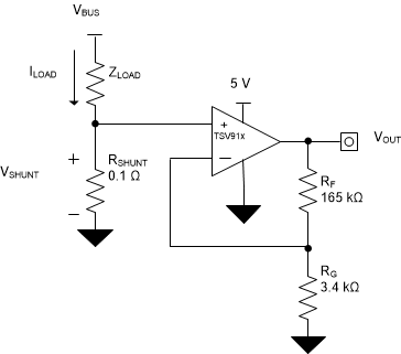
 Low-Side Motor Control
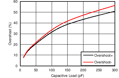
 Small-Signal Overshoot vs Load
Capacitance