SBOSA18C may 2020 – june 2023 TSV911A-Q1 , TSV912A-Q1 , TSV914A-Q1
PRODUCTION DATA
- 1
- 1 Features
- 2 Applications
- 3 Description
- 4 Revision History
- 5 Device Comparison Table
- 6 Pin Configuration and Functions
- 7 Specifications
- 8 Detailed Description
- 9 Application and Implementation
- 10Device and Documentation Support
- 11Mechanical, Packaging, and Orderable Information
Package Options
Mechanical Data (Package|Pins)
Thermal pad, mechanical data (Package|Pins)
Orderable Information
9.3.1 Input and ESD Protection
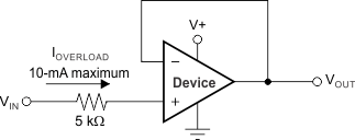
The TSV91xA-Q1 series incorporates internal ESD protection circuits on all pins. For input and output pins, this protection consists of current-steering diodes connected between the input and power-supply pins. These ESD protection diodes provide in-circuit, input overdrive protection, as long as the current is limited to 10-mA, as stated in the Absolute Maximum Ratings table. Figure 9-3 shows how a series input resistor is added to the driven input to limit the input current. The added resistor contributes thermal noise at the amplifier input and the value must be kept to a minimum in noise-sensitive applications.
 Figure 9-3 Input Current Protection