SLLSF15D August   2017  – May 2019 TUSB1042I

PRODUCTION DATA.  

  1. Features
  2. Applications
  3. Description
    1.     Device Images
      1.      Simplified Schematics
      2.      TUSB1042I Eye Diagram
  4. Revision History
  5. Pin Configuration and Functions
    1.     Pin Functions
  6. Specifications
    1. 6.1  Absolute Maximum Ratings
    2. 6.2  ESD Ratings
    3. 6.3  Recommended Operating Conditions
    4. 6.4  Thermal Information
    5. 6.5  Power Supply Characteristics
    6. 6.6  DC Electrical Characteristics
    7. 6.7  AC Electrical Characteristics
    8. 6.8  DCI Specific Electrical Characteristics
    9. 6.9  Timing Requirements
    10. 6.10 Switching Characteristics
    11. 6.11 Typical Characteristics
  7. Parameter Measurement Information
  8. Detailed Description
    1. 8.1 Overview
    2. 8.2 Functional Block Diagram
    3. 8.3 Feature Description
      1. 8.3.1 USB 3.1
      2. 8.3.2 4-level Inputs
      3. 8.3.3 Receiver Linear Equalization
    4. 8.4 Device Functional Modes
      1. 8.4.1 Device Configuration in GPIO Mode
      2. 8.4.2 Device Configuration In I2C Mode
      3. 8.4.3 Linear EQ Configuration
      4. 8.4.4 USB3.1 Modes
      5. 8.4.5 Operation Timing – Power Up
    5. 8.5 Programming
    6. 8.6 Register Maps
      1. 8.6.1 General Register (address = 0x0A) [reset = 00000001]
        1. Table 9. General Registers
      2. 8.6.2 USB3.1 Control/Status Registers (address = 0x20) [reset = 00000000]
        1. Table 10. USB3.1 Control/Status Registers (0x20)
      3. 8.6.3 USB3.1 Control/Status Registers (address = 0x21) [reset = 00000000]
        1. Table 11. USB3.1 Control/Status Registers (0x21)
      4. 8.6.4 USB3.1 Control/Status Registers (address = 0x22) [reset = 00000100]
        1. Table 12. USB3.1 Control/Status Registers (0x22)
  9. Application and Implementation
    1. 9.1 Application Information
    2. 9.2 Typical Application
      1. 9.2.1 Design Requirements
      2. 9.2.2 Detailed Design Procedure
      3. 9.2.3 Application Curve
    3. 9.3 System Examples
      1. 9.3.1 USB 3.1
  10. 10Power Supply Recommendations
  11. 11Layout
    1. 11.1 Layout Guidelines
    2. 11.2 Layout Example
  12. 12Device and Documentation Support
    1. 12.1 Related Links
    2. 12.2 Receiving Notification of Documentation Updates
    3. 12.3 Community Resources
    4. 12.4 Trademarks
    5. 12.5 Electrostatic Discharge Caution
    6. 12.6 Glossary
  13. 13Mechanical, Packaging, and Orderable Information

Package Options

Mechanical Data (Package|Pins)
Thermal pad, mechanical data (Package|Pins)
Orderable Information

Parameter Measurement Information

TUSB1042I Timing_Diagram_Definitions_SLLSEV7.gifFigure 9. I2C Timing Diagram Definitions
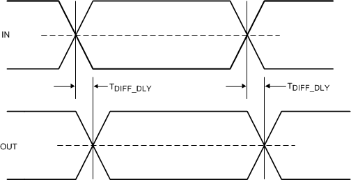
TUSB1042I Propagation_Delay_SLLSEV7.gifFigure 10. Propagation Delay
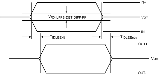
TUSB1042I Electrical_Idle_Mode_SLLSEV7.gifFigure 11. Electrical Idle Mode Exit and Entry Delay
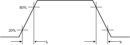
TUSB1042I Output_Rise_and_Fall_Times_SLLSEV7.gifFigure 12. Output Rise and Fall Times
TUSB1042I TUSB1046A_DCI_DCI_Clock_Propagation_Delay_SLLSF13.gifFigure 13. DCI Clock Propagation Delay