SLLSFP0 September 2024 TUSB1064-Q1
PRODUCTION DATA
- 1
- 1 Features
- 2 Applications
- 3 Description
- 4 Pin Configuration and Functions
- 5 Specifications
- 6 Parameter Measurement Information
- 7 Detailed Description
- 8 Application and Implementation
-
9 Register Maps
- 9.1 General Register (address = 0x0A) [reset = 00000001]
- 9.2 DisplayPort Control/Status Registers (address = 0x10) [reset = 00000000]
- 9.3 DisplayPort Control/Status Registers (address = 0x11) [reset = 00000000]
- 9.4 DisplayPort Control/Status Registers (address = 0x12) [reset = 00000000]
- 9.5 DisplayPort Control/Status Registers (address = 0x13) [reset = 00000000]
- 9.6 USB3.1 Control/Status Registers (address = 0x20) [reset = 00000000]
- 9.7 USB3.1 Control/Status Registers (address = 0x21) [reset = 00000000]
- 9.8 USB3.1 Control/Status Registers (address = 0x22) [reset = 00000000]
- 10Device and Documentation Support
- 11Revision History
- 12Mechanical, Packaging, and Orderable Information
Package Options
Mechanical Data (Package|Pins)
- RGF|40
Thermal pad, mechanical data (Package|Pins)
Orderable Information
3 Description
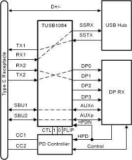
The TUSB1064-Q1 is a VESA® DisplayPort™ Alt Mode over USB-C® redriving switch that supports USB 3.2 data rates up to 10Gbps and DisplayPort 1.4 up to 8.1Gbps for upstream facing port (Sink). The device is used for UFP_D pin assignments C, D, and E from the VESA® DisplayPort™ Alt Mode over USB Type-C® Standard.
The TUSB1064-Q1 provides several levels of receive linear equalization to compensate for inter symbol interference (ISI) due to cable and board trace loss. The TUSB1064-Q1 operates on a single 3.3V supply and comes in an automotive grade 2 temperature range.
(1) For all available packages, see Section 12.
(2) The package size (length × width) is a nominal value and includes pins, where applicable.
 Simplified Schematics