SLLS413L February 2000 – June 2017 TUSB2046B , TUSB2046I
PRODUCTION DATA.
- 1 Features
- 2 Applications
- 3 Description
- 4 Revision History
- 5 Description (Continued)
- 6 Pin Configuration and Functions
- 7 Specifications
- 8 Detailed Description
- 9 Application and Implementation
- 10Power Supply Recommendations
- 11Layout
- 12Device and Documentation Support
- 13Mechanical, Packaging, and Orderable Information
Package Options
Mechanical Data (Package|Pins)
Thermal pad, mechanical data (Package|Pins)
- RHB|32
Orderable Information
8.3.2 Clock Generation
The input clock configuration logic of TUSB2046x is enhanced to accept a 6-MHz crystal or 48-MHz on-the-board clock source with a simple tie-off change on TSTMODE (pin 31).
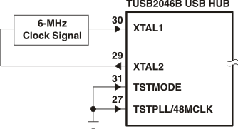
- A 6-MHz input clock configuration is shown in Figure 5.
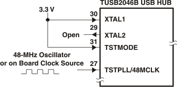
- A 48-MHz input clock configuration is shown in Figure 7.
In this mode, both TSTMODE and TSTPLL/48MCLK pins must be tied to ground. The hub is configured to use the 6-MHz clock on pins 30 and 29, which are XTAL1 and XTAL2, respectively, on the TUSB2046x. This is identical to the TUSB2046.
 Figure 5. 6-MHz Input Clock Configuration
NOTE:
This figure assumes a 6-MHz fundamental crystal that is parallel loaded. The component values of C1, C2, and Rd are determined using a crystal from Fox Electronics – part number HC49U-6.00MHz 30\50\0-70\20, which means ±30 ppm at 25°C and ±50 ppm from 0°C to 70°C. The characteristics for the crystal include a load capacitance (CL) of 20 pF, maximum shunt capacitance (Co) of 7 pF, and the maximum ESR of 50 Ω. In order to insure enough negative resistance, use C1 = C2 = 27 pF. The resistor Rd is used to trim the gain, and Rd = 1.5 kΩ is recommended.In this mode, both TSTMODE and XTAL1 pins must be tied to 3.3-V VCC. The hub accepts the 48-MHz clock input on TSTPLL/48MCLK (terminal 27). XTAL2 must be left floating (open) for this configuration. Only the oscillator or the onboard clock source is accepted for this mode. A crystal cannot be used for this mode, because the internal oscillator cell of the chip only supports the fundamental frequency.
 Figure 7. 48-MHz Input Clock Configuration