SLLSEX8B August 2017 – September 2017 TUSB215
PRODUCTION DATA.
- 1 Features
- 2 Applications
- 3 Description
- 4 Revision History
- 5 Pin Configuration and Functions
- 6 Specifications
- 7 Detailed Description
- 8 Application and Implementation
- 9 Power Supply Recommendations
- 10Layout
- 11Device and Documentation Support
- 12Mechanical, Packaging, and Orderable Information
Package Options
Refer to the PDF data sheet for device specific package drawings
Mechanical Data (Package|Pins)
- RGY|14
Thermal pad, mechanical data (Package|Pins)
Orderable Information
8 Application and Implementation
NOTE
Information in the following applications sections is not part of the TI component specification, and TI does not warrant its accuracy or completeness. TI’s customers are responsible for determining suitability of components for their purposes. Customers should validate and test their design implementation to confirm system functionality.
8.1 Application Information
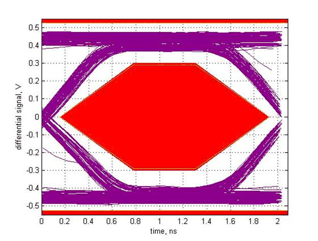
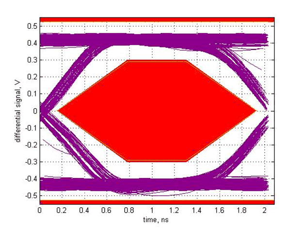
The primary purpose of the TUSB215 is to re-store the signal integrity of a USB High Speed channel up to the USB connector. The loss in signal quality stems from reduced channel bandwidth due to high loss PCB trace and other components that contribute a capacitive load. This can cause the channel to fail the USB near end eye mask. Proper use of the TUSB215 can help to pass this eye mask. Additionally the DC Boost helps overcoming DC losses from cables and traces.
A secondary purpose is to use the CD pin of the TUSB215 to control other blocks on the customer platform if so desired. The TUSB215 also provides CDP controller function.
8.2 Typical Application
A typical application is shown in Figure 6. In this setup, D2P and D2M face the USB connector while D1P and D1M face the USB host or hub. If desired, the orientation may be reversed [that is, D2 faces transceiver and D1 faces connector].
 Figure 6. Typical Application
8.2.1 Design Requirements
For this design example, use the parameters shown in the table below.
Table 3. Design Parameters
| PARAMETER | VALUE | |||
|---|---|---|---|---|
| VCC (4.4 V to 5.5 V) | 5 V | |||
| I2C support required in system (Yes/No) | No | |||
| AC Boost | REQ | Level | AC Boost Level 2: REQ = 3.83 k |
|
| 0-Ω | 0 | |||
| 1.69 k ±1% | 1 | |||
| 3.83 k ± 1% | 2 | |||
| DNI | 3 | |||
| DC Boost | RDC1 | RDC2 | Level | Mid DC Level: RDC1 = DNI RDC2 = DNI |
| 22 kΩ - 47 kΩ | Do Not Install (DNI) | 40 mV Low DC boost | ||
| DNI | DNI | 60 mV Mid DC boost | ||
| 47 kΩ | 24 kΩ | 80 mV High DC boost | ||
8.2.2 Detailed Design Procedure
TUSB215 requires a valid reset signal as described in the power supply recommendations section. The capacitor at RSTN pin is not required if a microcontroller drives the RSTN pin according to recommendations.
VREG pin is the internal LDO output that requires a 0.1-μF external capacitor to GND to stabilize the core.
The ideal AC boost setting is dependent upon the signal chain loss characteristics of the target platform. The general recommendation is to start with AC boost level 0, and then increment to AC boost level 1, etc. if permissible. Same applies to the DC Boost setting where it is recommended to plan for the required pads or connections to change boost settings, but to start with DC boost level 1.
In order for the TUSB215 to recognize any change to the AC and DC Boost settings, the RSTN pin must be toggled. This is because the configuration is latched on power up and the inputs are ignored thereafter.
NOTE
The TUSB215 compensates for DC attenuation in the signal path according to the configuration of the DC_BOOST pin. This pin is not 5V tolerant and therefore when selecting the highest DC boost level, the voltage level at DC_BOOST pin must be less than 3.6V.
Placement of the device is also dependent on the application goal. Table 4 summarizes our recommendations.
Table 4. Platform Placement Guideline
| PLATFORM GOAL | SUGGESTED DEVICE PLACEMENT |
|---|---|
| Pass USB Near End Mask | Close to measurement point |
| Pass USB Far End Eye Mask | Close to USB PHY |
| Cascade multiple devices to improve device enumeration | Midway between each USB interconnect |
 Figure 7. Reference Schematic
8.2.2.1 Test Procedure to Construct USB High Speed Eye Diagram
NOTE
USB-IF certification tests for High Speed eye masks require the mandated use of the USB-IF developed test fixtures. These test fixtures do not require the use of oscilloscope probes. Instead they use SMA cables. More information can be found at the USB-IF Compliance Updates Page. It is located under the ‘Electricals’ section, ID 86 dated March 2013.
The following procedure must be followed before using any oscilloscope compliance software to construct a USB High Speed Eye Mask:
8.2.2.1.1 For a Host Side Application
- Configure the TUSB215 to the desired AC and DC Boost settings
- Power on (or toggle the RSTN pin if already powered on) the TUSB215
- Using SMA cables, connect the oscilloscope and the USB-IF host-side test fixture to the TUSB215
- Enable the host to transmit USB TEST_PACKET
- Execute the oscilloscope USB compliance software.
- Repeat the above steps in order to re-test TUSB215 with a different settings
8.2.2.1.2 For a Device Side Application
- Configure the TUSB215 to the desired AC and DC Boost settings
- Power on (or toggle the RSTN pin if already powered on) the TUSB215
- Connect a USB host, the USB-IF device-side test fixture, and USB device to the TUSB215. Ensure that the USB-IF device test fixture is configured to the ‘INIT’ position
- Allow the host to enumerate the device
- Enable the device to transmit USB TEST_PACKET
- Using SMA cables, connect the oscilloscope to the USB-IF device-side test fixture and ensure that the device-side test fixture is configured to the ‘TEST’ position.
- Execute the oscilloscope USB compliance software.
- Repeat the above steps in order to re-test TUSB215 with a different settings
8.2.3 Application Curves
 Figure 8. Eye Diagram Bench Setup
 Figure 9. No TUSB215
 Figure 10. Low DC Boost, AC Boost Level 0
 Figure 12. High DC Boost, AC Boost Level 0
 Figure 14. Mid DC Boost, AC Boost Level 1
 Figure 16. Low DC Boost, AC Boost Level 2
 Figure 18. High DC Boost, AC Boost Level 2
 Figure 20. Mid DC Boost, AC Boost Level 3
 Figure 11. Mid DC Boost, AC Boost Level 0
 Figure 13. Low DC Boost, AC Boost Level 1
 Figure 15. High DC Boost, AC Boost Level 1
 Figure 17. Mid DC Boost, AC Boost Level 2
 Figure 19. Low DC Boost, AC Boost Level 3
 Figure 21. High DC Boost, AC Boost Level 3