SLLSEO5C October 2015 – May 2017 TUSB322I
PRODUCTION DATA.
- 1 Features
- 2 Applications
- 3 Description
- 4 Revision History
- 5 Pin Configuration and Functions
- 6 Specifications
-
7 Detailed Description
- 7.1 Overview
- 7.2 Functional Block Diagram
- 7.3 Feature Description
- 7.4 Device Functional Modes
- 7.5 Programming
- 7.6
Register Maps
- 7.6.1
CSR Registers
- 7.6.1.1 Device Identification Register (offset = 0x07 through 0x00) [reset = 0x00, 0x54, 0x55, 0x53, 0x42, 0x33, 0x32, 0x32]
- 7.6.1.2 Connection Status Register (offset = 0x08) [reset = 0x00]
- 7.6.1.3 Connection Status and Control Register (offset = 0x09) [reset = 0x20]
- 7.6.1.4 General Control Register (offset = 0x0A) [reset = 0x00]
- 7.6.1.5 Device Revision Register (offset = 0xA0) [reset = 0x02]
- 7.6.1
CSR Registers
- 8 Application and Implementation
- 9 Power Supply Recommendations
- 10Layout
- 11Device and Documentation Support
- 12Mechanical, Packaging, and Orderable Information
Package Options
Mechanical Data (Package|Pins)
- RWB|12
Thermal pad, mechanical data (Package|Pins)
Orderable Information
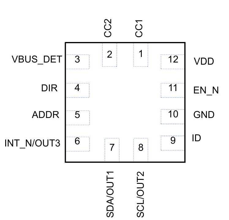
5 Pin Configuration and Functions
RWB Package
12-Pin X2QFN
Top View

Pin Functions
| PIN | I/O | DESCRIPTION | |
|---|---|---|---|
| NAME | NO. | ||
| CC1 | 1 | I/O | Type-C configuration channel signal 1 |
| CC2 | 2 | I/O | Type-C configuration channel signal 2 |
| VBUS_DET | 3 | I | 5-V to 28-V VBUS input voltage. VBUS detection determines UFP attachment. One 900-kΩ external resistor required between system VBUS and VBUS_DET pin. |
| DIR | 4 | O | DIR of plug. The open drain output indicates the detected plug orientation: Type-C plug position 2 (H); Type-C plug position 1 (L). |
| ADDR | 5 | I | Tri-level input pin to indicate I2C address or GPIO mode: H - I2C is enabled and I2C 7-bit address is 0x67. NC - GPIO mode (I2C is disabled) L - I2C is enabled and I2C 7-bit address is 0x47. ADDR pin should be pulled up to VDD if high configuration is desired |
| INT_N/OUT3 | 6 | O | The INT_N/OUT3 is a dual-function pin. When used as the INT_N, the pin is an open drain output in I2C control mode and is an active low interrupt signal for indicating changes in I2C registers. When used as OUT3, the pin is in audio accessory detect in GPIO mode: no detection (H), audio accessory connection detected (L). |
| SDA/OUT1 | 7 | I/O | The SDA/OUT1 is a dual-function pin. When I2C is enabled (ADDR pin is high or low), this pin is the I2C communication data signal. When in GPIO mode (ADDR pin is NC), this pin is an open drain output for communicating Type-C current mode detect when the TUSB322I device is in UFP mode: default current mode detected (H); medium or high current mode detected (L). |
| SCL/OUT2 | 8 | I/O | The SCL/OUT2 is a dual function pin. When I2C is enabled (ADDR pin is high or low), this pin is the I2C communication clock signal. When in GPIO mode (ADDR pin is NC), this pin is an open drain output for communicating Type-C current mode detect when the TUSB322I device is in UFP mode: default or medium current mode detected (H); high current mode detected (L). |
| ID | 9 | O | Open drain output; asserted low when the CC pins detect device attachment when port is a source (DFP), or dual-role (DRP) acting as source (DFP). |
| GND | 10 | G | Ground |
| EN_N | 11 | I | EN_N. Active low enable. |
| VDD | 12 | P | Positive supply voltage |