-
TUSB3410 USB to Serial Port Controller
- 1Device Overview
- 2Revision History
- 3Pin Configuration and Functions
- 4Specifications
-
5Detailed Description
- 5.1 Overview
- 5.2 Functional Block Diagram
- 5.3 Device Functional Modes
- 5.4 Processor Subsystems
- 5.5
Memory
- 5.5.1 MCU Memory Map
- 5.5.2 Registers
- 5.5.3 Buffers + I/O RAM Map
- 5.5.4
Endpoint Descriptor Block (EDB−1 to EDB−3)
- 5.5.4.1 OEPCNF_n: Output Endpoint Configuration (n = 1 to 3) (Base Addr: FF08h, FF10h, FF18h)
- 5.5.4.2 OEPBBAX_n: Output Endpoint X-Buffer Base Address (n = 1 to 3) (Offset 1)
- 5.5.4.3 OEPBCTX_n: Output Endpoint X Byte Count (n = 1 to 3) (Offset 2)
- 5.5.4.4 OEPBBAY_n: Output Endpoint Y-Buffer Base Address (n = 1 to 3) (Offset 5)
- 5.5.4.5 OEPBCTY_n: Output Endpoint Y-Byte Count (n = 1 to 3) (Offset 6)
- 5.5.4.6 OEPSIZXY_n: Output Endpoint X-/Y-Buffer Size (n = 1 to 3) (Offset 7)
- 5.5.4.7 IEPCNF_n: Input Endpoint Configuration (n = 1 to 3) (Base Addr: FF48h, FF50h, FF58h)
- 5.5.4.8 IEPBBAX_n: Input Endpoint X-Buffer Base Address (n = 1 to 3) (Offset 1)
- 5.5.4.9 IEPBCTX_n: Input Endpoint X-Byte Count (n = 1 to 3) (Offset 2)
- 5.5.4.10 IEPBBAY_n: Input Endpoint Y-Buffer Base Address (n = 1 to 3) (Offset 5)
- 5.5.4.11 IEPBCTY_n: Input Endpoint Y-Byte Count (n = 1 to 3) (Offset 6)
- 5.5.4.12 IEPSIZXY_n: Input Endpoint X-/Y-Buffer Size (n = 1 to 3) (Offset 7)
- 5.5.4.13 Endpoint-0 Descriptor Registers
- 5.5.5
USB Registers
- 5.5.5.1 FUNADR: Function Address Register (Addr:FFFFh)
- 5.5.5.2 USBSTA: USB Status Register (Addr:FFFEh)
- 5.5.5.3 USBMSK: USB Interrupt Mask Register (Addr:FFFDh)
- 5.5.5.4 USBCTL: USB Control Register (Addr:FFFCh)
- 5.5.5.5 MODECNFG: Mode Configuration Register (Addr:FFFBh)
- 5.5.5.6 Clock Output Control
- 5.5.5.7 Vendor ID/Product ID
- 5.5.5.8 SERNUM7: Device Serial Number Register (Byte 7) (Addr:FFEFh)
- 5.5.5.9 SERNUM6: Device Serial Number Register (Byte 6) (Addr:FFEEh)
- 5.5.5.10 SERNUM5: Device Serial Number Register (Byte 5) (Addr:FFEDh)
- 5.5.5.11 SERNUM4: Device Serial Number Register (Byte 4) (Addr:FFECh)
- 5.5.5.12 SERNUM3: Device Serial Number Register (Byte 3) (Addr:FFEBh)
- 5.5.5.13 SERNUM2: Device Serial Number Register (Byte 2) (Addr:FFEAh)
- 5.5.5.14 SERNUM1: Device Serial Number Register (Byte 1) (Addr:FFE9h)
- 5.5.5.15 SERNUM0: Device Serial Number Register (Byte 0) (Addr:FFE8h)
- 5.5.5.16 Function Reset and Power-Up Reset Interconnect
- 5.5.5.17 Pullup Resistor Connect and Disconnect
- 5.5.6
DMA Controller Registers
- 5.5.6.1 DMACDR1: DMA Channel Definition Register (UART Transmit Channel) (Addr:FFE0h)
- 5.5.6.2 DMACSR1: DMA Control And Status Register (UART Transmit Channel) (Addr:FFE1h)
- 5.5.6.3 DMACDR3: DMA Channel Definition Register (UART Receive Channel) (Addr:FFE4h)
- 5.5.6.4 DMACSR3: DMA Control And Status Register (UART Receive Channel) (Addr:FFE5h)
- 5.5.7
UART Registers
- 5.5.7.1 RDR: Receiver Data Register (Addr:FFA0h)
- 5.5.7.2 TDR: Transmitter Data Register (Addr:FFA1h)
- 5.5.7.3 LCR: Line Control Register (Addr:FFA2h)
- 5.5.7.4 FCRL: UART Flow Control Register (Addr:FFA3h)
- 5.5.7.5 Transmitter Flow Control
- 5.5.7.6 MCR: Modem-Control Register (Addr:FFA4h)
- 5.5.7.7 LSR: Line-Status Register (Addr:FFA5h)
- 5.5.7.8 MSR: Modem-Status Register (Addr:FFA6h)
- 5.5.7.9 DLL: Divisor Register Low Byte (Addr:FFA7h)
- 5.5.7.10 DLH: Divisor Register High Byte (Addr:FFA8h)
- 5.5.7.11 Baud-Rate Calculation
- 5.5.7.12 XON: Xon Register (Addr:FFA9h)
- 5.5.7.13 XOFF: Xoff Register (Addr:FFAAh)
- 5.5.7.14 MASK: UART Interrupt-Mask Register (Addr:FFABh)
- 5.5.8 Expanded GPIO Port
- 5.5.9 Interrupts
- 5.5.10 I2C Registers
- 5.6
Boot Modes
- 5.6.1 Introduction
- 5.6.2 Bootcode Programming Flow
- 5.6.3 Default Bootcode Settings
- 5.6.4 External I2C Device Header Format
- 5.6.5 Checksum in Descriptor Block
- 5.6.6 Header Examples
- 5.6.7 USB Host Driver Downloading Header Format
- 5.6.8 Built-In Vendor Specific USB Requests
- 5.6.9 Bootcode Programming Consideration
- 5.6.10 File Listings
- 6Application, Implementation, and Layout
- 7Device and Documentation Support
- 8Mechanical Packaging and Orderable Information
- IMPORTANT NOTICE
Package Options
Mechanical Data (Package|Pins)
Thermal pad, mechanical data (Package|Pins)
- RHB|32
Orderable Information
DATA SHEET
TUSB3410 USB to Serial Port Controller
1 Device Overview
1.1 Features
- Fully Compliant With USB 2.0 Full-Speed Specifications: TID#40340262
- Supports 12-Mbps USB Data Rate (Full Speed)
- Supports USB Suspend, Resume, and Remote Wake-Up Operations
- Configurable to Bus-Powered and Self-Powered Operation
- Supports a Total of Three Input and Three Output (Interrupt, Bulk) Endpoints
- Integrated 8052 Microcontroller With:
- 256 × 8 RAM for Internal Data
- 10K × 8 ROM (With USB and I2C Bootloader)
- 16K × 8 RAM for Code Space Loadable From Host or I2C Port
- 2K × 8 Shared RAM Used for Data Buffers and Endpoint Descriptor Blocks (EDBs)
- Master I2C Controller for EEPROM Device Access
- MCU Operates at 24 MHz, Providing 2-MIPS Operation
- 128-ms Watchdog Timer
- Enhanced UART Features:
- Software and Hardware Flow Control
- Automatic RS-485 Bus Transceiver Control, With and Without Echo
- Selectable IrDA Mode for Up to 115.2-kbps Transfer
- Software-Selectable Baud Rate From 50 BPS to 921.6 kbps
- Programmable Serial-Interface Characteristics
- 5-, 6-, 7-, or 8-Bit Characters
- Even, Odd, or No Parity-bit Generation and Detection
- 1-, 1.5-, or 2-Stop Bit Generation
- Line Break Generation and Detection
- Internal Test and Loopback Capabilities
- Modem Control Functions (CTS, RTS, DSR, RI and DCD)
- Internal Diagnostic Capability
- Loopback Control for Communications
Link-Fault Isolation - Break, Parity, Overrun, Framing-Error Simulation
- Loopback Control for Communications
1.2 Applications
- Modems
- Peripherals:
Printers, Handheld Devices, and so on - Medical Meters
- DSP and µC Interface
1.3 Description
The TUSB3410 device provides bridging between a USB port and an enhanced UART serial port. The device contains an 8052 microcontroller unit (MCU) with 16KB of RAM that can be loaded from the host or from the external onboard memory through an I2C. The device also contains 10KB of ROM that allows the MCU to configure the USB port at boot time. The ROM code also contains an I2C bootloader. All device functions (such as the USB command decoding, UART setup, and error reporting) are managed by the internal MCU firmware in unison with the PC host.
Device Information(1)
| PART NUMBER | PACKAGE | BODY SIZE |
|---|---|---|
| TUSB3410 | VQFN (32) | 5.00 mm × 5.00 mm |
| LQFP (32) | 7.00 mm × 7.00 mm |
- For all available packages, see the orderable addendum at the end of the data sheet.
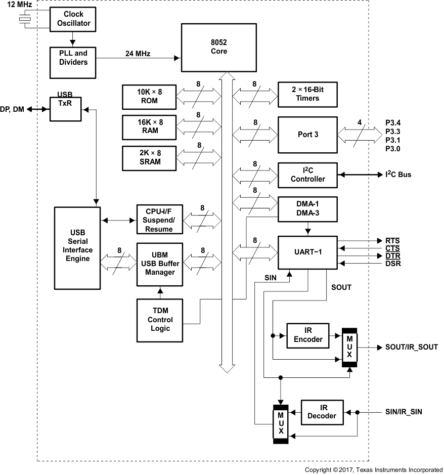
1.4 Functional Block Diagram

2 Revision History
Changes from I Revision (November 2015) to J Revision
- Changed pin 21 From: DTR To: active low DTR in the Pin Functions tableGo
- Changed the description of bit 7 CONT in USBCTL: USB Control Register (Addr:FFFCh), CONT= 0 From: enabled To: disables, CONT= 1 From: disbaled To: enabledGo
Changes from H Revision (April 2013) to I Revision
- Added Pin Configuration and Functions section, ESD Ratings table, Thermal Information table, Typical Characteristics section, Feature Description section, Device Functional Modes, Application and Implementation section, Power Supply Recommendations section, Layout section, Device and Documentation Support section, and Mechanical, Packaging, and Orderable Information section Go
- Deleted Ordering Information table.Go
3 Pin Configuration and Functions
3.1 Pin Diagrams
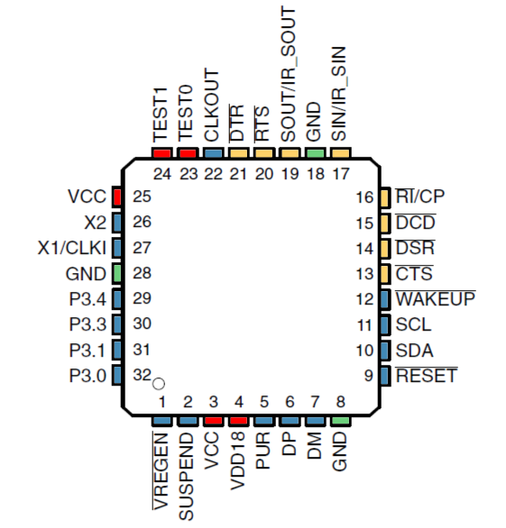
RHB Package
32-Pin VQFN
Top View

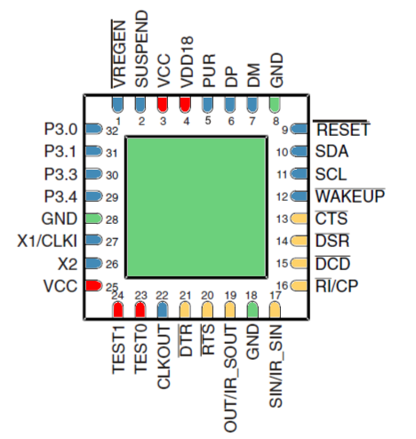
VF Package
32-Pin LQFP
Bottom View

Pin Functions
| PIN | I/O | DESCRIPTION | |
|---|---|---|---|
| NAME | NO. | ||
| CLKOUT | 22 | O | Clock output (controlled by bits 2 (CLKOUTEN) and 3(CLKSLCT) in the MODECNFG register (see (1) and Section 5.5.5.5) |
| CTS | 13 | I | UART: Clear to send(4) |
| DCD | 15 | I | UART: Data carrier detect(4) |
| DM | 7 | I/O | Upstream USB port differential data minus |
| DP | 6 | I/O | Upstream USB port differential data plus |
| DSR | 14 | I | UART: Data set ready(4) |
| DTR | 21 | O | UART: Data terminal ready(1) |
| GND | 8, 18, 28 | GND | Digital ground |
| P3.0 | 32 | I/O | General-purpose I/O 0 (port 3, terminal 0)(3)(5)(8) |
| P3.1 | 31 | I/O | General-purpose I/O 1 (port 3, terminal 1)(3)(5)(8) |
| P3.3 | 30 | I/O | General-purpose I/O 3 (port 3, terminal 3)(3)(5)(8) |
| P3.4 | 29 | I/O | General-purpose I/O 4 (port 3, terminal 4)(3)(5)(8) |
| PUR | 5 | O | Pullup resistor connection(2) |
| RESET | 9 | I | Device master reset input(4) |
| RI/CP | 16 | I | UART: Ring indicator(4) |
| RTS | 20 | O | UART: Request to send(1) |
| SCL | 11 | O | Master I2C controller: clock signal(1) |
| SDA | 10 | I/O | Master I2C controller: data signal(1)(5) |
| SIN/IR_SIN | 17 | I | UART: Serial input data / IR Serial data input(6) |
| SOUT/IR_SOUT | 19 | O | UART: Serial output data / IR Serial data output(7) |
| SUSPEND | 2 | O | Suspend indicator terminal(3). When this terminal is asserted high, the device is in suspend mode. |
| TEST0 | 23 | I | Test input (for factory test only). This terminal must be tied to VCC through a 10-kΩ resistor. |
| TEST1 | 24 | I | Test input (for factory test only)(5). This terminal must be tied to VCC through a 10-kΩ resistor. |
| VCC | 3, 25 | PWR | 3.3 V |
| VDD18 | 4 | PWR | 1.8-V supply. An internal voltage regulator generates this supply voltage when terminal VREGEN is low. When VREGEN is high, 1.8 V must be supplied externally. |
| VREGEN | 1 | I | This active-low terminal is used to enable the 3.3-V to 1.8-V voltage regulator. |
| WAKEUP | 12 | I | Remote wake-up request terminal. When low, wakes up system(5) |
| X1/CLKI | 27 | I | 12-MHz crystal input or clock input |
| X2 | 26 | O | 12-MHz crystal output |
(1) 3-state CMOS output (±4-mA drive and sink)
(2) 3-state CMOS output (±8-mA drive and sink)
(3) 3-state CMOS output (±12-mA drive and sink)
(4) TTL-compatible, hysteresis input
(5) TTL-compatible, hysteresis input, with internal 100-µA active pullup resistor
(6) TTL-compatible input without hysteresis, with internal 100-µA active pullup resistor
(7) Normal or IR mode: 3-state CMOS output (±4-mA drive and sink)
(8) The MCU treats the outputs as open drain types in that the output can be driven low continuously, but a high output is driven for two clock cycles and then the output is high impedance.