SLLSEI1C July 2015 – July 2024 TUSB4020BI-Q1
PRODUCTION DATA
- 1
- 1 Features
- 2 Applications
- 3 Description
- 4 Pin Configuration and Functions
- 5 Specifications
-
6 Detailed Description
- 6.1 Overview
- 6.2 Functional Block Diagram
- 6.3 Feature Description
- 6.4 Device Functional Modes
- 6.5 Programming
- 6.6
Register Maps
- 6.6.1
Configuration Registers
- 6.6.1.1 ROM Signature Register (offset = 0h) [reset = 0h]
- 6.6.1.2 Vendor ID LSB Register (offset = 1h) [reset = 51h]
- 6.6.1.3 Vendor ID MSB Register (offset = 2h) [reset = 4h]
- 6.6.1.4 Product ID LSB Register (offset = 3h) [reset = 25h]
- 6.6.1.5 Product ID MSB Register (offset = 4h) [reset = 80h]
- 6.6.1.6 Device Configuration Register (offset = 5h) [reset = 1Xh]
- 6.6.1.7 Battery Charging Support Register (offset = 6h) [reset = 0Xh]
- 6.6.1.8 Device Removable Configuration Register (offset = 7h) [reset = 0Xh]
- 6.6.1.9 Port Used Configuration Register (offset = 8h) [reset = 0h]
- 6.6.1.10 PHY Custom Configuration Register (offset = 9h) [reset = 0h]
- 6.6.1.11 Device Configuration Register 2 (offset = Ah)
- 6.6.1.12 UUID Registers (offset = 10h to 1Fh)
- 6.6.1.13 Language ID LSB Register (offset = 20h)
- 6.6.1.14 Language ID MSB Register (offset = 21h)
- 6.6.1.15 Serial Number String Length Register (offset = 22h)
- 6.6.1.16 Manufacturer String Length Register (offset = 23h)
- 6.6.1.17 Product String Length Register (offset = 24h)
- 6.6.1.18 Serial Number Registers (offset = 30h to 4Fh)
- 6.6.1.19 Manufacturer String Registers (offset = 50h to 8Fh)
- 6.6.1.20 Product String Registers (offset = 90h to CFh)
- 6.6.1.21 Additional Feature Configuration Register (offset = F0h)
- 6.6.1.22 Charging Port Control Register (offset = F2h)
- 6.6.1.23 Device Status and Command Register (offset = F8h)
- 6.6.1
Configuration Registers
- 7 Application and Implementation
- 8 Power Supply Recommendations
- 9 Layout
- 10Device and Documentation Support
- 11Revision History
- 12Mechanical, Packaging, and Orderable Information
Package Options
Mechanical Data (Package|Pins)
- PHP|48
Thermal pad, mechanical data (Package|Pins)
- PHP|48
Orderable Information
3 Description
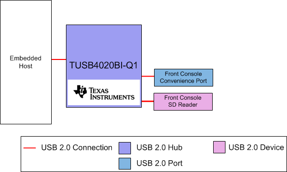
The TUSB4020BI-Q1 is a two-port USB 2.0 hub, which provides USB high-speed/full-speed connections on the upstream port and high-speed, full-speed, or low-speed connections on the two downstream ports. When the upstream port is connected to an electrical environment that supports high-speed and full-speed/low-speed connections, high-speed and full-speed/low-speed USB connectivity is enabled on the downstream ports. When the upstream port is connected to an electrical environment that only supports full-speed/low-speed connections, high-speed connectivity are disabled on the downstream ports.
The TUSB4020BI-Q1 supports per port or ganged power switching and overcurrent protection.
An individually port power controlled hub switches power on or off to each downstream port as requested by the USB host. Also when an individually port power controlled hub senses an overcurrent event, only power to the affected downstream port is switched off.
A ganged hub switches on power to all the downstream ports when power is required to be on for any port. The power to the downstream ports is not switched off unless all ports are in a state that allows power to be removed. Also when a ganged hub senses an overcurrent event, power to all downstream ports is switched off.
The TUSB4020BI-Q1 provides terminal strap configuration for some features (including battery charging support) and customization through OTP ROM, I2C EEPROM or an I2C/SMBus target interface for PID, VID, custom port and phy configurations. Custom string support is also available when using an I2C EEPROM or the I2C/SMBus target interface.
The device is available in a 48-pin HTQFP package and is designed for operation over the industrial temperature range of –40°C to 85°C.
 Block Diagram