SLLSET3 May 2016 TUSB501-Q1
PRODUCTION DATA.
- 1 Features
- 2 Applications
- 3 Description
- 4 Revision History
- 5 Device Comparison Table
- 6 Pin Configuration and Functions
- 7 Specifications
- 8 Parameter Measurement Information
- 9 Detailed Description
- 10Application and Implementation
- 11Power Supply Recommendations
- 12Layout
- 13Device and Documentation Support
- 14Mechanical, Packaging, and Orderable Information
Package Options
Mechanical Data (Package|Pins)
- DRF|8
Thermal pad, mechanical data (Package|Pins)
- DRF|8
Orderable Information
1 Features
- Q100 Automotive Qualified
- Aggressive Low-Power Architecture (Typical):
- 126 mW Active Power
- 20 mW in U2/U3
- 4 mW with No Connection
- Automatic LFPS DE Control
- Excellent Jitter and Loss Compensation
- 32 inches of FR4 4 mil Stripline
- 3 m of 30 AWG cable
- Integrated Termination
- Small 2 x 2 mm QFN Package
- Selectable Receiver Equalization, Transmitter De-Emphasis and Output Swing
- Hot-Plug Capable
- ESD Protection ±5 kV HBM and 1500 V CDM
2 Applications
- Cell Phones
- Computers
- Docking Stations
- TVs
- Active Cables
- Backplanes
3 Description
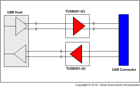
The TUSB501-Q1 is a 3rd generation 3.3-V USB 3.0 single-channel redriver. When 5 Gbps SuperSpeed USB signals travel across a PCB or cable, signal integrity degrades due to loss and inter-symbol interference. The TUSB501-Q1 recovers incoming data by applying equalization that compensates channel loss, and drives out signals with a high differential voltage. This extends the possible channel length, and enables systems to pass USB 3.0 compliance. The TUSB501-Q1 advanced state machine makes it transparent to hosts and devices.
After power up, the TUSB501-Q1 periodically performs receiver detection on the TX pair. If it detects a SuperSpeed USB receiver, RX termination becomes enabled, and the TUSB501-Q1 is ready to redrive.
The receiver equalizer has three gain settings that are controlled by pin EQ: 3 dB, 6 dB, and 9 dB. This should be set based on amount of loss before the TUSB501-Q1. Likewise, the output driver supports configuration of De-Emphasis and Output Swing (pins DE and OS). These settings allow the TUSB501-Q1 to be flexibly placed in the SuperSpeed USB path, with optimal performance.
Over previous generations, the TUSB501-Q1 features reduced power in all link states, a stronger OS option, improved receiver equalization settings, and an intelligent LFPS Controller. This controller senses the low frequency signals and automatically disables driver de-emphasis, for full USB 3.0 compliance.
The TUSB501-Q1 is packaged in a small 2 x 2 mm QFN, and operates through an industrial temperature range of –40°C to 105°C.
Device Information(1)
| PART NUMBER | PACKAGE | BODY SIZE (NOM) |
|---|---|---|
| TUSB501-Q1 | WSON | 2.00 mm x 2.00 mm |
- For all available packages, see the orderable addendum at the end of the data sheet.
Simple Application
