SLLSEZ0E April 2017 – April 2018 TUSB544
PRODUCTION DATA.
- 1 Features
- 2 Applications
- 3 Description
- 4 Revision History
- 5 Pin Configuration and Functions
- 6 Specifications
-
7 Detailed Description
- 7.1 Overview
- 7.2 Functional Block Diagram
- 7.3 Feature Description
- 7.4 Device Functional Modes
- 7.5 Programming
- 7.6
Register Maps
- 7.6.1
TUSB544 Registers
- 7.6.1.1 GENERAL_4 Register (Offset = Ah) [reset = 1h]
- 7.6.1.2 GENERAL_5 Register (Offset = Bh) [reset = 0h]
- 7.6.1.3 GENERAL_6 Register (Offset = Ch) [reset = 0h]
- 7.6.1.4 DISPLAYPORT_1 Register (Offset = 10h) [reset = 0h]
- 7.6.1.5 DISPLAYPORT_2 Register (Offset = 11h) [reset = 0h]
- 7.6.1.6 DISPLAYPORT_3 Register (Offset = 12h) [reset = 0h]
- 7.6.1.7 DISPLAYPORT_4 Register (Offset = 13h) [reset = 0h]
- 7.6.1.8 DISPLAYPORT_5 Register (Offset = 1Bh) [reset = 0h]
- 7.6.1.9 USB3.1_1 Register (Offset = 20h) [reset = 0h]
- 7.6.1.10 USB3.1_2 Register (Offset = 21h) [reset = 0h]
- 7.6.1.11 USB3.1_3 Register (Offset = 22h) [reset = 0h]
- 7.6.1.12 USB3.1_4 Register (Offset = 23h) [reset = 23h]
- 7.6.1
TUSB544 Registers
- 8 Application and Implementation
- 9 Power Supply Recommendations
- 10Layout
- 11Device and Documentation Support
- 12Mechanical, Packaging, and Orderable Information
Package Options
Mechanical Data (Package|Pins)
- RNQ|40
Thermal pad, mechanical data (Package|Pins)
Orderable Information
6.9 Switching Characteristics
over operating free-air temperature range (unless otherwise noted)| PARAMETER | TEST CONDITIONS | MIN | TYP | MAX | UNIT | |
|---|---|---|---|---|---|---|
| AUXP/N and SBU1/2 | ||||||
| tAUX_PD | Switch propagation delay | 400 | ps | |||
| tAUX_SW_OFF | Switching time CTL1 to switch OFF | Not including tCTL1_DEBOUNCE | 500 | ns | ||
| tAUX_SW_ON | Switching time CTL1 to switch ON | 500 | ns | |||
| tAUX_INTRA | Intra-pair output skew | 100 | ps | |||
| USB3.1 and DisplayPort mode transition requirement GPIO mode | ||||||
| tGP_USB_4DP | Min overlap of CTL1 and CTL1 when transitioning from USB 3.1 only mode to 4-Lane DisplayPort mode or vice versa. | 4 | µs | |||
| CTL1 and HPDIN | ||||||
| tCTL1_DEBOUNCE | CTL1 and HPDIN debounce time when transitioning from H to L. | DP Lanes will be disabled if low for greater than min value. | 3 | ms | ||
| I2C (Refer to Figure 1) | ||||||
| fSCL | I2C clock frequency | 1 | MHz | |||
| tBUF | Bus free time between START and STOP conditions | 0.5 | µs | |||
| tHDSTA | Hold time after repeated START condition. | After this period, the first clock pulse is generated | 0.26 | µs | ||
| tLOW | Low period of the I2C clock | 0.5 | µs | |||
| tHIGH | High period of the I2C clock | 0.26 | µs | |||
| tSUSTA | Setup time for a repeated START condition | 0.26 | µs | |||
| tHDDAT | Data hold time | 0 | μs | |||
| tSUDAT | Data setup time | 50 | ns | |||
| tR | Rise time of both SDA and SCL signals | 120 | ns | |||
| tF | Fall time of both SDA and SCL signals | 20 × (VI2C/5.5 V) | 120 | ns | ||
| tSUSTO | Setup time for STOP condition | 0.26 | μs | |||
| Cb | Capacitive load for each bus line | 100 | pF | |||
 Figure 1. I2C Timing Diagram Definitions
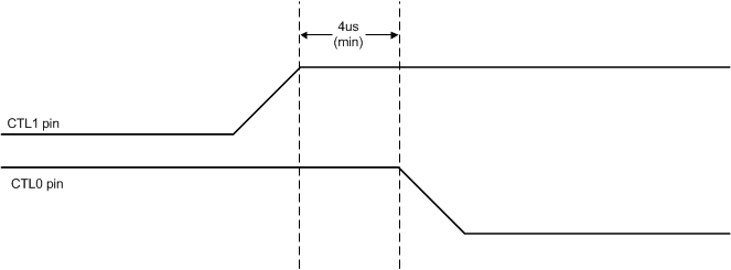 Figure 2. USB3.1 to 4-Lane DisplayPort in GPIO Mode
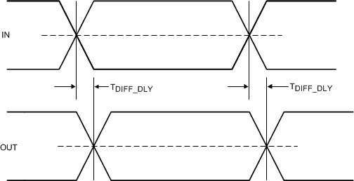 Figure 3. Propagation Delay
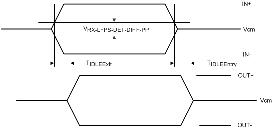 Figure 4. Electrical Idle Mode Exit and Entry Delay
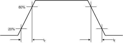 Figure 5. Output Rise and Fall Times
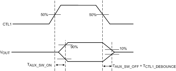 Figure 6. AUX and SBU Switch ON and OFF Timing Diagram