SLLSEV7E August 2016 – March 2023 TUSB546-DCI
PRODUCTION DATA
- 1 Features
- 2 Applications
- 3 Description
- 4 Revision History
- 5 Pin Configuration and Functions
- 6 Specifications
-
7 Detailed Description
- 7.1 Overview
- 7.2 Functional Block Diagram
- 7.3 Feature Description
- 7.4 Device Functional Modes
- 7.5 Programming
- 7.6
Register Maps
- 7.6.1 General Register (address = 0x0A) [reset = 00000001]
- 7.6.2 DisplayPort Control/Status Registers (address = 0x10) [reset = 00000000]
- 7.6.3 DisplayPort Control/Status Registers (address = 0x11) [reset = 00000000]
- 7.6.4 DisplayPort Control/Status Registers (address = 0x12) [reset = 00000000]
- 7.6.5 DisplayPort Control/Status Registers (address = 0x13) [reset = 00000000]
- 7.6.6 USB3.1 Control/Status Registers (address = 0x20) [reset = 00000000]
- 7.6.7 USB3.1 Control/Status Registers (address = 0x21) [reset = 00000000]
- 7.6.8 USB3.1 Control/Status Registers (address = 0x22) [reset = 00000100]
- 8 Application and Implementation
- 9 Device and Documentation Support
- 10Mechanical, Packaging, and Orderable Information
Package Options
Mechanical Data (Package|Pins)
- RNQ|40
Thermal pad, mechanical data (Package|Pins)
Orderable Information
3 Description
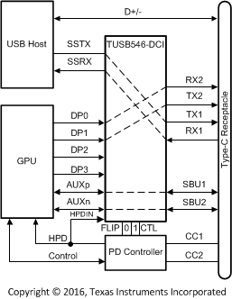
The TUSB546-DCI is a VESA USB Type-C™ Alt Mode redriving switch supporting USB 3.1 data rates up to 5 Gbps and DisplayPort 1.4 up to 8.1 Gbps for downstream facing port (Host). The device is used for configurations C, D, E, and F from the VESA DisplayPort Alt Mode on USB Type-C Standard Version 1.1. This protocol-agnostic linear redriver is also capable of supporting other USB Type-C Alt Mode interfaces.
The TUSB546-DCI provides several levels of receive linear equalization to compensate for cable and board trace loss due to inter symbol interference (ISI). Operates on a single 3.3 V supply and comes in a commercial temperature range and industrial temperature range.
| PART NUMBER | PACKAGE | BODY SIZE (NOM) |
|---|---|---|
| TUSB546-DCI | RNQ (WQFN, 40) | 4.00 mm × 6.00 mm |
| TUSB546I-DCI |
 Simplified Schematics
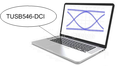
 TUSB546-DCI Eye
Diagram