SLLSEE5D february 2013 – july 2023 TUSB8040A1
PRODUCTION DATA
- 1
- 1Features
- 2Applications
- 3Description
- 4Revision History
- 5Pin Configuration and Functions
- 6Specifications
-
7Detailed Description
- 7.1 Overview
- 7.2 Functional Block Diagram
- 7.3 Memory
- 7.4 I2C EEPROM Operation
- 7.5 SMBus Target Operation
- 7.6
Configuration Registers
- 7.6.1 ROM Signature Register
- 7.6.2 Vendor ID LSB Register
- 7.6.3 Vendor ID MSB Register
- 7.6.4 Product ID LSB Register
- 7.6.5 Product ID MSB Register
- 7.6.6 Device Configuration Register
- 7.6.7 Battery Charging Support Register
- 7.6.8 Device Removable Configuration Register
- 7.6.9 Port Used Configuration Register
- 7.6.10 Reserved Register
- 7.6.11 Reserved Register
- 7.6.12 Language ID LSB Register
- 7.6.13 Language ID MSB Register
- 7.6.14 Serial Number String Length Register
- 7.6.15 Manufacturer String Length Register
- 7.6.16 Product String Length Register
- 7.6.17 Reserved Register
- 7.6.18 Serial Number Registers
- 7.6.19 Manufacturer String Registers
- 7.6.20 Product String Registers
- 7.6.21 Additional Feature Configuration Register
- 7.6.22 Reserved Register
- 7.6.23 Reserved Register
- 7.6.24 Device Status and Command Register
-
8Applications, Implementation, and Layout
- 8.1 Application Information
- 8.2
Typical Application
- 8.2.1 Design Requirements
- 8.2.2
Detailed Design Procedure
- 8.2.2.1 Upstream Port Implementation
- 8.2.2.2 Downstream Port 1 Implementation
- 8.2.2.3 Downstream Port 2 Implementation
- 8.2.2.4 Downstream Port 3 Implementation
- 8.2.2.5 Downstream Port 4 Implementation
- 8.2.2.6 VBUS Power Switch Implementation
- 8.2.2.7 Clock, Reset, I2C/SMBUS, and Misc
- 8.2.2.8 Power Implementation
- 8.2.3 Application Curve
- 8.2.4 Power Supply Recommendations
- 8.2.5
Layout
- 8.2.5.1
Layout Guidelines
- 8.2.5.1.1 Part Placement
- 8.2.5.1.2
Board Layout Considerations
- 8.2.5.1.2.1 RKM Package – QFN (Quad Flat No-Lead)
- 8.2.5.1.2.2 Impedance
- 8.2.5.1.2.3 Critical Signals
- 8.2.5.1.2.4 Crystal
- 8.2.5.1.2.5 USB Interface
- 8.2.5.1.2.6 Differential Pair Signals
- 8.2.5.1.2.7 Port Connectors
- 8.2.5.1.2.8 Reset Terminals
- 8.2.5.1.2.9 Miscellaneous Terminals
- 8.2.5.1.2.10 Power Control and Battery Charging Terminals
- 8.2.5.1.2.11 USB 2.0 Port Indicator LED Terminals
- 8.2.5.1.3 Power
- 8.2.5.2 Layout Example
- 8.2.5.1
Layout Guidelines
- 9Device and Documentation Support
- Mechanical, Packaging, and Orderable Information
Package Options
Mechanical Data (Package|Pins)
- RKM|100
Thermal pad, mechanical data (Package|Pins)
- RKM|100
Orderable Information
3 Description
The TUSB8040A1 is a four-port USB 3.0 compliant hub and is available in a 100-pin WQFN package. The device is designed for operation over the commercial temperature range of 0°C to 70°C.
The TUSB8040A1 provides simultaneous SuperSpeed USB and high-speed or full-speed connections on the upstream port and provides SuperSpeed USB, high-speed, full-speed, or low-speed connections on the downstream ports. When the upstream port is connected to an electrical environment that only supports high-speed, full-speed, or low-speed connections, SuperSpeed USB connectivity is disabled on the downstream ports. When the upstream port is connected to an electrical environment that only supports full-speed or low-speed connections, SuperSpeed USB and high-speed connectivity are disabled on the downstream ports.
The TUSB8040A1 supports up to four downstream ports. The device may be configured to report one to four downstream ports by pin selection or by an attached EEPROM or SMBus controller. The configuration options provide the ability to scale the device by application.
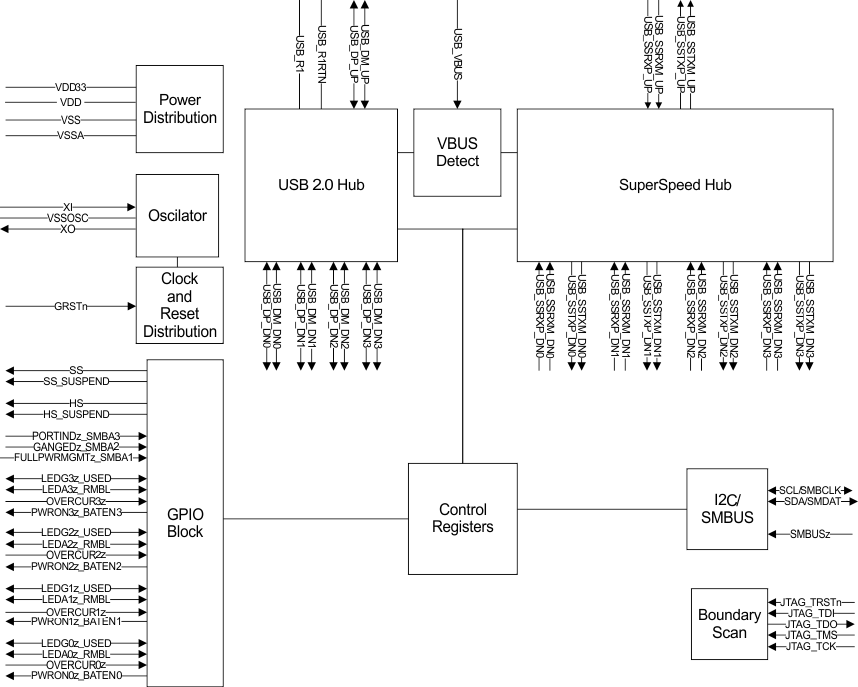
Figure 8-1 shows a typical view of the TUSB8040A1.
 Functional Block Diagram